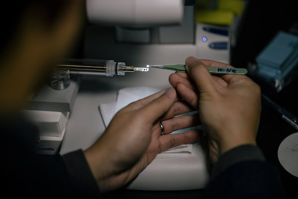
[Image above] Purdue postdoctoral research associate Jie Jian mounts a ceramic sample for research using a transmission electron microscope. Credit: Purdue University; Erin Easterling
When it comes to ceramics, sintering is an integral part of processing.
And while the process of sintering is rather complex, the idea behind it is simple—using heat to meld individual ceramic particles into a solid body.
Sintering works, and works well, but one drawback is that sintering requires a lot of heat and a lot of time—typically conditions of ~1,500ºC for several hours are required to sinter ceramics.
And in manufacturing, a lot of energy and a lot of time translates into higher costs.
Which is precisely why techniques such as cold sintering and field-assisted sintering techniques, such as flash sintering—which can drastically reduce processing times and temperatures—are extremely interesting to manufacturers and beyond.
Flash sintering uses an electric field to reduce ceramic processing times by about 50%—lowering the amount of energy required and speeding up the process to altogether reduce manufacturing costs.
We know that flash sintering works. We understand the process macroscopically. And although we have theories about the mechanisms that make flash sintering work—such as thermal runaway—the precise nanoscale and microscale phenomena that happen within ceramic materials during sintering are not well understood.
So a collaboration of researchers from Purdue University and beyond is using a $3 million grant to take an up close look at flash sintering in a massive effort to broaden applications of the technique. Using a combination of in situ and modeling techniques, the team is aiming to characterize the nano-and micro-scale events that happen during flash sintering in a variety of ceramic materials.
Haiyan Wang, Basil S. Turner Professor of Engineering in Purdue’s School of Materials Engineering, will lead the project, which also includes Edwin García and Xinghang Zhang from Purdue University; Amiya Mukherjee, distinguished professor of materials science and engineering at UC Davis; Thomas Tsakalakos, distinguished professor of materials science and engineering at Rutgers; Troy Holland, assistant professor of mechanical engineering at Colorado State University; and C. Stephen Hellberg, Noam Bernstein, and Steven Erwin, physicists at the Naval Research Laboratory.
The U.S. Office of Naval Research grant will fund the team’s study of flash sintering over the next four years.

Haiyan Wang, center, reviews a TEM image with doctoral student Xuejing Wang, left, and postdoctoral research associate Jie Jian. Credit: Purdue University; Charles Jischke
“Our scope is to understand why within a matter of seconds and at such a low temperature you can facilitate sintering, which conventionally needs a much longer time at higher temperature,” Wang says in a Purdue press release. “Despite successful demonstrations of flash sintering, it remains poorly understood at the atomic scale.”
To get at those atomic scale details, the scientists will probe mechanical properties of ceramic materials during different sintering conditions. Using in situ methods to simulate what happens ex situ, the scientists will carefully dissect how an electrical field and heat affect a material’s microstructure during flash sintering.
Although Wang says there are various possibilities to explain how flash sintering works—such as Joule heating, ion transport, and dielectric breakdown—we don’t yet understand the fundamental mechanism or mechanisms of flash sintering.
In particular, some hypotheses suggest that grain boundary effects are key to flash sintering, so the team will precisely probe grain boundary dynamics during flash sintering using conventional TEM, in situ TEM, and in situ XTEM microscopy. Using these microscopy tools, the team will watch what happens in the ceramics’ crystal structure during sintering, using real-time video to capture the small scale of sintering.
“These techniques can provide valuable information about what’s really happening at grain boundaries,” Wang explains.
But that’s just part of the project.

Jie Jian places a sample under the microscope for analysis. Credit: Purdue University

Close-up of the ceramic sample. Credit: Purdue University
“The first step is to understand the mechanism through detailed grain boundary studies,” Wang says. “The second step is to use that understanding to design ceramic materials to meet functionality needs, and to use flash sintering to sinter those materials.”
That’s where the modeling comes in. The scientists will use their newfound understanding of the process to develop simulations that will help other scientists pinpoint flash sintering conditions for a particular material. “This is a strong part of the proposal—we are going to use both in situ experiments and modeling simulations to create a sort of feedback loop,” Wang says.
She explains that understanding how and why the technique works will help researchers apply flash sintering to other materials that are more difficult to process. Those materials may require a higher power supply, longer processing times, or higher temperatures during flash sintering—and Wang and her team want to understand why and how to help facilitate flash sintering in those materials, she says, to broaden applications of flash sintering.
The team will study several different types of materials during flash sintering. “We are going to look at ion-conducting materials, such as gadolinium-doped ceria and yttria-stabilized zirconia, but also nonionic conductors like titanium dioxide and barium titanate. On top of that, we’re also going to look at difficult to flash materials like alumina, for which flash it theoretically possible but the conditions are difficult,” Wang says.
And, on top of all that, those different types of materials may use different mechanisms during flash sintering—all of which Wang and her team hope to elucidate.
For instance, she says, oxygen vacancies at grain boundaries may be critical during flash sintering of ion-conducting materials, while charge carriers may be pertinent in electrically conducting materials.
By understanding how different types of materials respond to flash sintering, the team wants to use simulations to develop a set of guidelines to help choose flash sintering conditions by simply knowing a material’s composition.
“We can’t understand everything, but we hope that the combined efforts with collaborators can help the community understand a better way to flash sintering,” Wang says.
Hear more about the project from Wang and her Purdue team in the short video below.