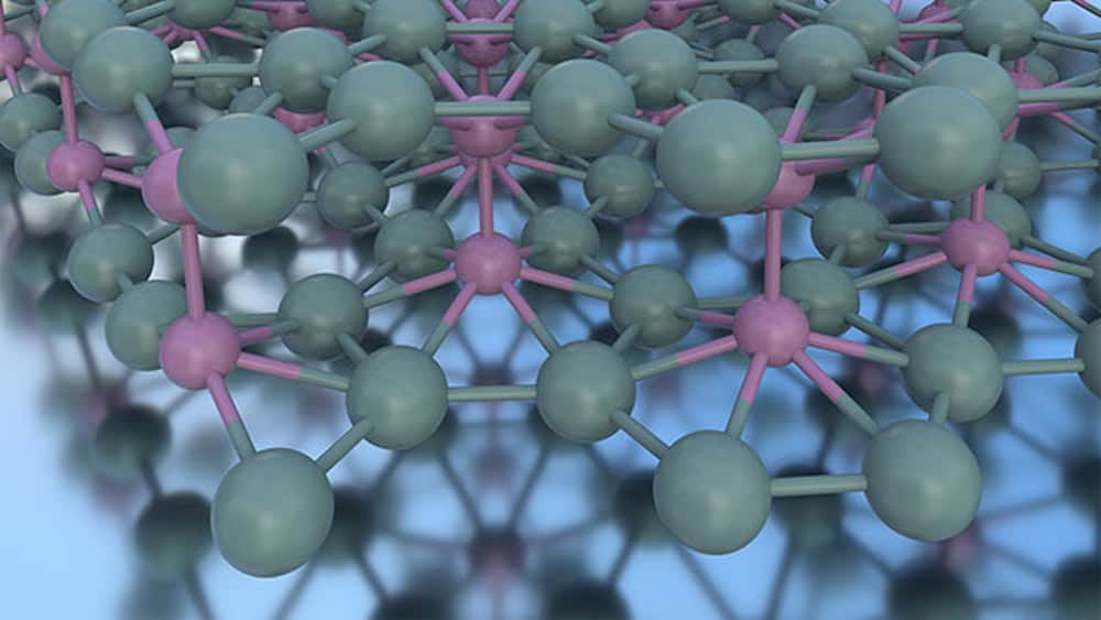
[Image above] Atomic structure of bilayer borophene. All atoms are boron; pink boron atoms are involved in bonding the two layers. Credit: Mark C. Hersam, Northwestern University
When you hear the term “2D material,” you likely imagine a material that consists of a single layer of atoms. However, this mental image is not necessarily correct—as long as the thickness of a material is constrained within the nanoscale, a few-layered material can still be called 2D.
Graphene, for example, can be up to 10 layers thick and still be called “graphene” because the electrical properties remain distinct from those of the bulk form, according to the International Organization for Standardization.
When reviewing studies on 2D materials, then, you cannot take it for granted that the material consists of a single layer. The 2D material borophene is an exception.
Borophene is a 2D sheet of boron atoms that is similar to graphene—both are flexible, strong, and lightweight, though borophene is even more so. Unlike graphene, however, only single-atomic-layer borophene has been experimentally realized.
“When you try to grow a thicker layer, the boron wants to adopt its bulk structure, [which unlike graphite is not layered.] Rather than remaining atomically flat, thicker boron films form particles and clusters,” says Mark C. Hersam, Walter P. Murphy Professor of Materials Science and Engineering at Northwestern University, in a university press release.
Hersam is co-senior author on a new study by researchers at Northwestern and Rice Universities. In their study, they suggest a way to overcome the clustering tendency of boron atoms, which they discovered following a “serendipitous observation” when growing borophene on a flat, silver substrate.
“When exposed to very high temperatures, the silver bunched to form exceptionally flat, large terraces between bunches of atomic-scale steps,” the press release explains. These terraces promoted random nucleation of the borophene, leading to the formation of a second layer. When the researchers noticed this formation, they focused their efforts on improving second layer growth.
The paper details how they fine-tuned the method to grow bilayer borophene, which includes
- Annealing the silver substrate at 650°C. Annealing at such high temperatures guarantees the formation of flat silver terraces with a typical width exceeding 1 μm. As a result, “the majority of the borophene nucleation sites are on terraces instead of along step edges, which have a stronger templating effect in aligning domains than terrace.”
- Performing electron-beam evaporation of a pure boron rod onto the substrate at 350–450°C. Growth of bilayer borophene is favored at these relatively low temperatures, “where only mixed-phase (v1/5 and v1/6 borophene) and pure v1/6 borophene grow.”
After growing the bilayer borophene, the researchers imaged the samples using in situ scanning tunnelling microscopy and noncontact atomic force microscopy. They then compared these atomic-scale spatial resolution images with density functional theory calculations to determine the borophene structure.
They determined that the borophene consists of two sparsely covalently bonded α-phase layers. In addition, through field-emission resonance spectroscopy, they showed that the bilayer borophene exhibits superior crystallinity and a heightened work function compared to single-atomic-layer borophene. Taken together, these properties give bilayer borophene great potential for use in energy or chemical storage applications.
In the press release, Hersam says he hopes the study will inspire other researchers to grow even thicker layers of borophene or create double layers with different atomic geometries.
“Diamonds, graphite, graphene and carbon nanotubes are all based on one element (carbon) with different geometries. Boron appears to be just as rich in its possibilities, if not more so, than carbon. We believe that we are still in the early chapters of the two-dimensional boron saga,” he says.
The paper, published in Nature Materials, is “Borophene synthesis beyond the single-atomic-layer limit” (DOI: 10.1038/s41563-021-01084-2).
Author
Lisa McDonald
CTT Categories
- Material Innovations
- Nanomaterials


