[Image above] Schematic shows how to make core/shell nanowire solar cell starting from left with a CdS nanowire (green) that is dipped in CuCl where cation exchange reaction creates a Cu2S shell coating (brown). Metal contacts are then deposited on the CdS core and Cu2S shell. Credit: Yang et. al.
By sheer coincidence, I received information about two different methods of using nanowires to boost efficiency and/or lower the cost of solar cells. Generally speaking, the use of nanowires is intriguing because of the possibilities to improve photovoltaic performances by, for example, providing more light absorption area, broadening the photon collection spectrum (by using an optimizing mix of nanowire compositions), improving antireflectivity and decreasing active materials and processing costs. Nevertheless, the real life performance of nanowire-based PV cells has been disappointing for the most part. These new announcements, however, suggest that progress on this front is still being made.
One of the new approaches comes from a Swedish company, Sol Voltaics, which claims to have a novel production method that “combines the low cost and substrate versatility of thin films with the high conversion efficiency of III-V materials.”
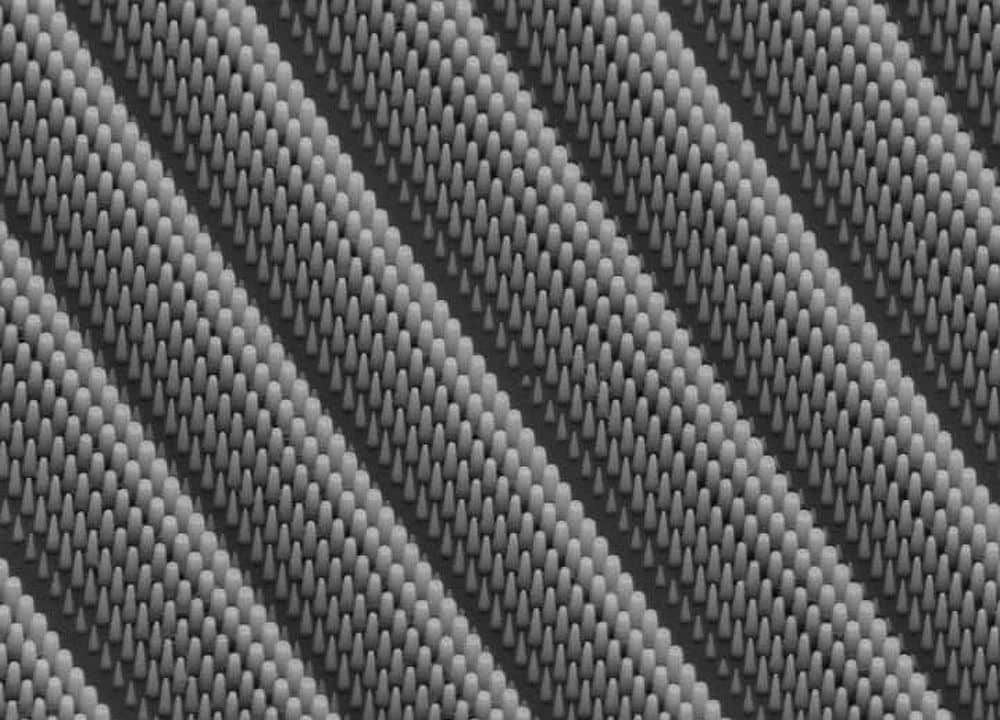
 from the side and (e) cross section. Credit: Sol Voltaics.")
GaN–GaInP core-shell nanowire (d) from the side and (e) cross section. Credit: Sol Voltaic
In brief, Sol Voltaics claims two key abilities. The first is that instead of growing nanowires in expensive reactor batches, the company says it knows how to produce self-assembling type III-V nanowires in a continuous gas phase flow process. The second is that the resultant nanowires can be applied to a substrate immediately and directly from the aerosol flow process, or stored in a liquid or as a dry powder for use at another time. Sol Voltaics says the self-assembled arrays of the nanowires are dense and can be “contacted in parallel to form a solar panel of any size.”
It should be noted that previously the company had learned how to use metal organic vapor phase epitaxy to produce multijunction nanowires and also to create a variety of structures including nanotrees and core–shell heterostructures. Lars Samuelson, CSO and cofounder of Sol Voltaics (itself a spin off of the Nanometer Structure Consortium of Lund University), and several other investigators recently reported in the IEEE Journal of Selected Topics in Quantum Electronics (doi:10.1109/JSTQE.2010.2073681) that they had been successful with a highly efficient set-up of III-V multijunction nanowires grown epitaxially on silicon wafers instead of pricier germanium substrates. Further, the company implies that it is making headway in producing multijunction nanowires through the use of its gas phase production approach.
Speaking of core-shell nanowires, researchers at the Lawrence Berkeley National Lab say that they have also developed a low cost approach to producing photovoltaic materials. The LBL team, led by Peidong Yang, says it has learned how to make core-shell nanowires by a three step process. They first make nanowires from cadmium sulfide. Next, these are partially dipped in copper sulfide for several minutes. Finally separate metal contacts are applied to both the CdS core and the resultant Cu2S shell.
For both Sol Voltaics and the LBL group, the core-shell concept is of interest because it provides a radial p-n junction, with each individual nanowire serving as a photovoltaic cell and greatly improved the light-trapping capabilities of silicon-based photovoltaic thin films.
The nanowire dipping approach being used at LBL is based on previous work by Paul Alvisatos, someone whom we have written about several times in the past.
In a news release, Yang says “The initial cadmium sulfide nanowires were synthesized by physical vapor transport using a vapor–liquid–solid mechanism rather than wet chemistry, which gave us better quality material and greater physical length, but certainly they can also be made using solution process. The as-grown single-crystalline cadmium sulfide nanowires have diameters of between 100 and 400 nanometers and lengths up to 50 millimeters.”
Although Yang doesn’t mention Sol Voltaics, he goes on to suggest, it appears, that his group’s approach may be superior to at least some aerosol methods. He says, “The solution-based cation exchange reaction provides us with an easy, low-cost method to prepare high-quality hetero-epitaxial nanomaterials. Furthermore, it circumvents the difficulties of high-temperature doping and deposition for typical vapor phase production methods, which suggests much lower fabrication costs and better reproducibility. All we really need are beakers and flasks for this solution-based process. There’s none of the high fabrication costs associated with gas-phase epitaxial chemical vapor deposition and molecular beam epitaxy, the techniques most used today to fabricate semiconductor nanowires.”