[Image above] Credit: UT Dallas; Vimeo
The scanning tunneling microscope (STM) won its designers, Heinrich Rohrer and Gerd Binnig, the Nobel Prize in Physics in 1986.
But even more impressive than the fact that the microscopy technique has earned one of the highest honors in the scientific world (or is it?) is what STM can actually do—it creates a sort of topographical map for the surface of a material. But in this landscape, the mountains and valleys are on the scale of individual atoms.
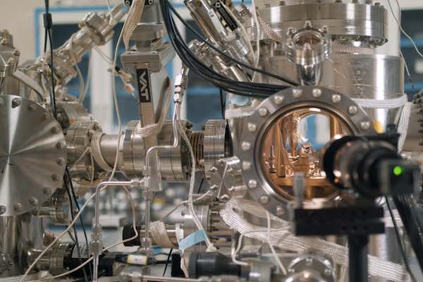
The idea behind the method the microscope uses is simple enough. An STM has a probe tip affixed to a cantilever arm—which is free to swing up and down—that reads the surface structure of a material like a hand reading braille, feeling its way across 3-D surface features.
The cantilever traces the surface, guided by an electrical signal that forms between the material surface and probe tip as electrons tunnel between the two.
Despite its atomic utility, however, STM has a problem in practice—the probe tip has a tendency to crash into the surface of the material it’s measuring, damaging both in the process. It interrupts data collection, it’s a pain, and it’s expensive.
In an effort to improve STM, however, researchers at the University of Texas at Dallas now have a solution—they have pinpointed the problem that allows a tip to crash into the sample it’s scanning and have devised a way to prevent it from happening.
Their analysis found that a controller that regulates the position of the STM probe can have a hard time keeping up with surface irregularities, which can prevent the tip from moving evenly across the surface.
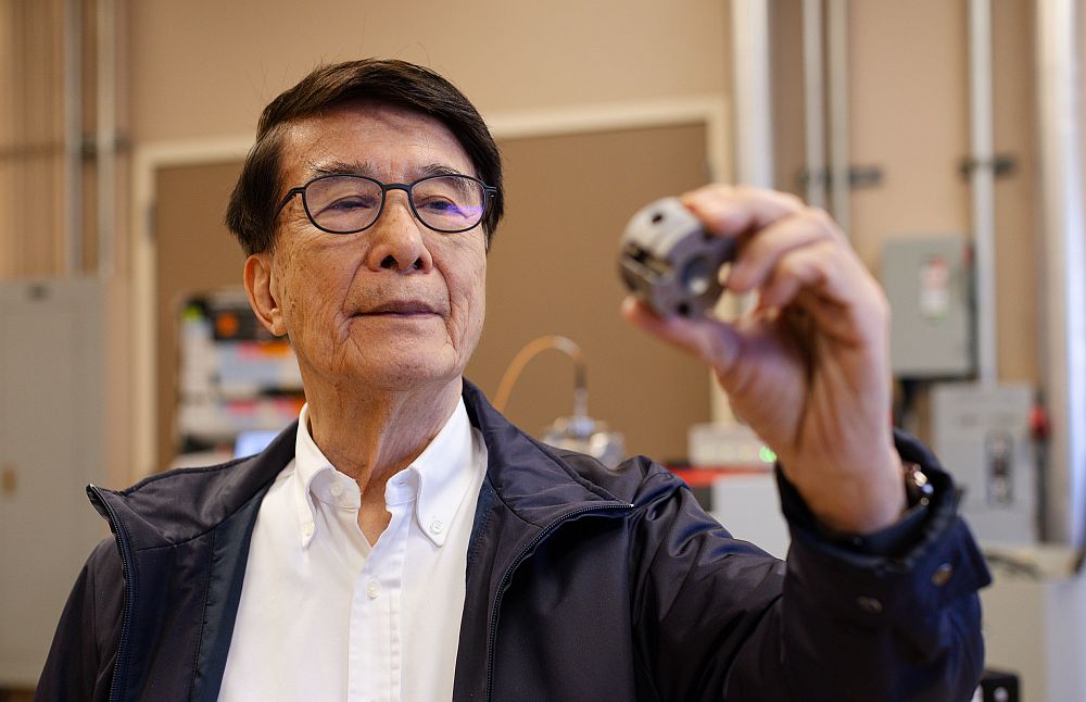
“There’s a feedback controller in the STM that measures the current and moves the needle up and down,” Reza Moheimani, professor of mechanical engineering at the University of Texas at Dallas, explains in a UT Dallas news release. “You’re moving from one atom to another, across an uneven surface. It is not flat. Because of that, the distance between the sample and tip changes, as does the current between them. While the controller tries to move the tip up and down to maintain the current, it does not always respond well, nor does it regulate the tip correctly. The resulting movement of the tip is often unstable.”
When you’re going for atomic level precision, unstable is not good. So Moheimani and a team of researchers, including mechanical engineering graduate student Farid Tajaddodianfar, developed an algorithm that helps the controller more accurately adjust the probe tip in real time, as it moves along the surface.
“He [Tajaddodianfar] figured out a way of measuring that local barrier height and adjusting the gain on the control system that demonstrably keeps the tip out of trouble,” John Randall, adjunct professor at UT Dallas and president of nanotechnology company Zyvex Labs, says in the release. “Without it, the tip just bumps along, crashing into the surface. Now, it adjusts to the control parameters on the fly.”
And with a focus on ever-more precise manufacturing of ever-more compact devices, it’s more important than ever to have atomic precision. The ability to accurately measure the atomic composition of a material, atom by atom, is critical for such atomic architecture of structures.
“By building structures atom by atom, you’re able to create new, extraordinary materials,” Randall says in the release. “We can remove impurities and make materials stronger and more heat resistant. We can build quantum computers. It could radically lower costs and expand capabilities in medicine and other areas. For example, if we can better understand DNA at an atomic and molecular level, that will help us fine-tune and tailor health care according to patients’ needs. The possibilities are endless.”
The paper describing their work, published in Review of Scientific Instruments, is “On the effect of local barrier height in scanning tunneling microscopy: Measurement methods and control implications” (10.1063/1.5003851)
See more about the technique and the scientists who developed it in the short video below.
Credit: UT Dallas; Vimeo
Did you find this article interesting? Subscribe to the Ceramic Tech Today newsletter to continue to read more articles about the latest news in the ceramic and glass industry! Visit this link to get started.
Author
April Gocha
CTT Categories
- Material Innovations
- Nanomaterials


