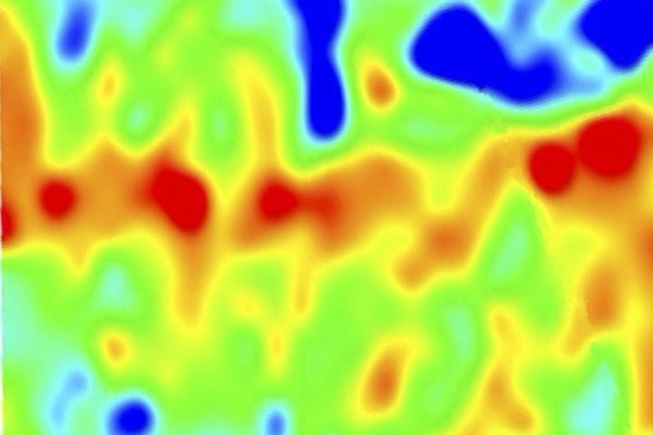
[Image above] 3-D atomic stoichiometry obtained from APT allows quantification of 3-D charge distribution and thus voltage at the grain boundary. Credit: David Diercks; Brian Gorman
Editor’s note: This story originally appeared in print in the May 2016 ACerS Bulletin.
For such a small thing, grain boundaries are big.
Grain boundaries—the spaces in between grains of a polycrystalline material—are defects, so it’s no surprise that they have important consequences on the material that they reside within.
“Grain boundaries are important because they dominate the properties of many ceramics—this is inconvenient because grain boundaries typically make up only a fraction of the volume compared with the bulk volume,” Brian Gorman, associate professor of metallurgical and materials engineering at Colorado School of Mines, explains via email.
Grain boundaries influence a host of material attributes, including a material’s thermal, electrical, optical, magnetic, and mechanical properties. In other words, these tiny defects critically contribute to how a material behaves in this world.
Gorman and a team of researchers at Colorado School of Mines and the University of Florida are well on their way to solving grain boundaries’ secrets, however—the team recently achieved unprecedented atom-by-atom visualization of the chemical composition of grain boundaries.
In addition to providing beautiful maps of the atoms that reside at grain boundaries, the results provide direct insight into how local charges influence a material’s ionic conductivity—results that could help tune a material’s nanoscale composition to optimize macroscale properties.
The work, recently reported in the Journal of Materials Chemistry A, describes how the team used atom probe tomography (APT) to 3-D quantify oxygen and cation compositions at grain boundaries within a polycrystalline material.
APT uses a laser to evaporate atoms from a sharp-tipped sample of material, using a position sensitive detector to resolve individual atoms with high detection efficiency. While APT previously has been used to quantify grain boundaries in metallic materials, its application to oxide materials has been less straightforward.
But not anymore—the team 3-D-quantified impurity cations and oxygen stoichiometry with sub-nanometer resolution in Nd-doped ceria, a material with important energy applications (particularly in fuel cells).
Beyond this impressive feat of atomic resolution, the team also quantified space charge voltage at grain boundaries and related it to ionic conductivity. In other words, the scientists showed that they can directly correlate structural measurements to material properties. “This ‘closes the loop’ on processing–structure–property relationships,” Gorman says.
The results represent the first time that researchers have measured 3-D oxygen stoichiometry at sub-nanometer spatial resolution—information that can associate defect chemistry at the nanoscale, which again ties together with macroscale properties, Gorman adds.

(left) Brightfield TEM image of the atom probe specimen showing the grain boundary, overlaid onto an APT data reconstruction locating Si impurities at the boundary. (center) A 3-D volume reconstruction (and corresponding 1-D composition profile, below) from APT data illustrates excess Nd dopants and sub-stoichiometric O at the grain boundary. (right) 3-D atomic stoichiometry obtained from APT allows quantification of 3-D charge distribution and thus voltage at the grain boundary. Credit: David Diercks; Brian Gorman
But the results didn’t come overnight.
“In order to accomplish this work we had to first prove that we could determine oxygen concentrations quantitatively using laser-assisted atom probe tomography. We accomplished this over several years and, using experimental data, tied in to finite element models of the atom probe experiment.”
But the scientists didn’t stop there. They did their due diligence, making sure that they were on the right track.
Gorman continues, “We also had to prove that the oxygen stoichiometry changes we were observing were indeed associated with grain boundaries, so we performed correlative transmission electron microscopy [TEM] imaging before and after APT experiments—again which we have been working on for more than 8 years. Finally, we put together mathematical formalisms to convert 3-D APT data first into charge distributions and then into voltage distributions using a 3-D solution to the Poisson equation.”
In the end, the scientists’ results were big, although a bit unexpected. According to Gorman, they were surprised by how well the APT structure data matched transport measurements and literature values (e.g., for quantities like Ce3+/Ce4+ ratios).
Altogether, the results give the team confidence that what they have is the real deal. “We are now very comfortable with the whole process and believe we can analyze grain boundaries in virtually any oxide,” Gorman says.
Although the team is confident that the technique can be applied to other materials, that doesn’t mean the application will necessarily be easy. “Unfortunately, every material behaves differently in the atom probe, so every material presents its own challenges,” Gorman adds.
But, he says, the team thinks that the challenges can be overcome in most cases.
“And with future hardware developments, we should be capable of improving these results even further and reducing the challenges to APT experiments. In the next few years, we may see the combination of TEM and APT demonstrating not only sub-nanometer spatial resolution, but true atomic lattice resolution—and possibly even with the ability to visualize individual point defects,” Gorman speculates.
The paper, published in the Journal of Materials Chemistry A, is “Three-dimensional quantification of composition and electrostatic potential at individual grain boundaries in doped ceria” (DOI: 10.1039/C5TA10064J).
Author
April Gocha
CTT Categories
- Basic Science
- Energy
- Material Innovations
- Modeling & Simulation
- Nanomaterials


