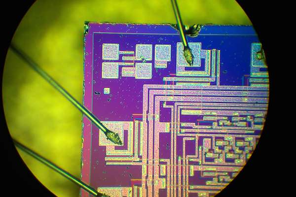
[Image above] Credit: Jasper Nance; Flickr CC BY-NC-ND 2.0
Are silicon’s days on top of the semiconductor world numbered?
Other materials are certainly vying for their place in the spotlight. Who can blame them? Although the global semiconductor market is experiencing a slight decline of late, overall market annual spending is still in the $60-billion range.
For instance, last year I reported on how gallium nitride was trying to use violence to take the crown. And a brand new single crystal fabrication method developed by Lehigh University scientists may now allow more materials to vie for top semiconductor status.
But that’s not all.
ORNL scientists now report on a new processing technique that could help bring 2-D electronic devices to the forefront, establishing a “path to replace silicon as the choice for semiconductors in some applications,” according to an ORNL press release.
“Everyone is looking for the next material—the thing that will replace silicon for transistors,” Alex Belianinov, lead author of the new research, says in the release. “2-D devices stand out as having low power consumption and being easier and less expensive to fabricate without requiring harsh chemicals that are potentially harmful to the environment.”
2-D devices are so attractive because they offer promise of low power, high efficiency, and mechanical flexibility, all of which could mean better devices that use less power.
And if a heavy dose of funding is a sign of a particularly promising area of research, then 2-D materials have that going for them, too.
So what’s the new secret to 2-D?
Using an atomic sandblaster, the ORNL scientists tailored the properties of the bulk ferroelectric material copper indium thiophosphate.
“Our method opens pathways to direct-write and edit circuitry on 2-D material without the complicated current state-of-the-art multistep lithographic processes,” lead researcher Olga Ovchinnikova says in the release.

Diagram illustrates the effect of helium ions on the mechanical and electrical properties of the layered ferroelectric: a) Disappearance domains in the exposed area; as the mound forms yellow regions (ferroelectricity) gradually disappear; b) Mechanical properties of the material; warmer colors indicate hard areas, cool colors indicate soft areas; c) Conductivity enhancement; warmer colors show insulating areas, cooler colors show more conductive areas. Credit: ORNL
The so-called sandblaster is a helium ion microscope, which is usually used to cut and shape materials. Instead, the researchers used it to “control ferroelectric domain distribution, enhance conductivity, and grow nanostructures” according to the release.
See more about the ORNL research in the short video below.

Credit: Oak Ridge National Laboratory; YouTube
The paper, published in ACS Applied Materials & Interfaces, is “Polarization control via He-ion beam induced nanofabrication in layered ferroelectric semiconductors” (DOI: 10.1021/acsami.5b12056).
Rice University researchers also believe in 2-D materials, although they’re betting on the theoretical potential of flat boron. Their work shows that 2-D boron is a natural low-temperature superconductor and may be the sole 2-D material that can claim such fame.
Although the new work is theoretical rather than experimental, it shows that calculations predict that 2-D boron is metallic and will conduct electrons without resistance at cold temperatures (between 10 and 20 kelvin type of cold).
“It’s well-known that the material is pretty light because the atomic mass is small,” research scientists and first author Evgeni Penev says in a Rice press release. “If it’s metallic too, these are two major prerequisites for superconductivity. That means at low temperatures, electrons can pair up in a kind of dance in the crystal.”
Rice theoretical physicist and senior author Boris Yakobson adds, “Lower dimensionality is also helpful. It may be the only, or one of very few, two-dimensional metals. So there are three factors that gave the initial motivation for us to pursue the research. Then we just got more and more excited as we got into it.”
That paper, published in Nano Letters, is “Can two-dimensional boron superconduct?” (DOI: 10.1021/acs.nanolett.6b00070).
Still not happy with those material choices?
Perhaps transition metal dichalcogenides are more your thing. If so, you might be intrigued to know that resurgence of traditional synthesis methods, such as chemical and physical vapor deposition, are making few-atom-thick crystals of these materials possible—and opening up processing routes to new 2-D materials with promising properties for future optical, electronic, and mechanical devices.
For a full overview of that technology, see the review paper published in Applied Materials Today: “From bulk crystals to atomically thin layers of group VI-transition metal dichalcogenides vapour phase synthesis” (DOI: 10.1016/j.apmt.2015.12.003).
Do you have other ideas about materials that are poised to overtake the semiconductor industry?