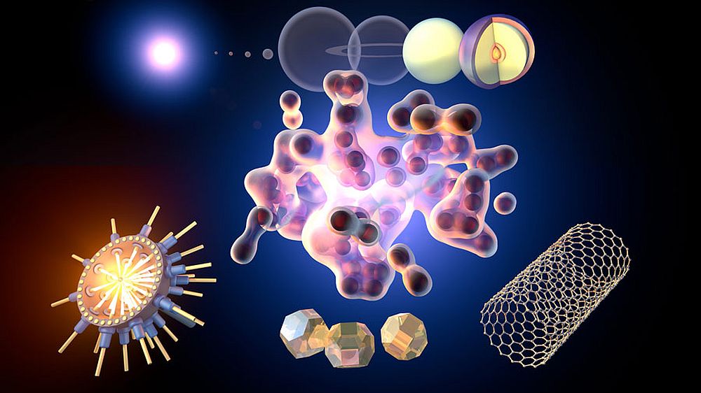
[Image above] Hexagonal boron nitride may one day replace diamond as the go-to material for quantum systems. Credit: University of Technology Sydney
Though the quantum world as it is portrayed in television shows and movies stretches reality, scientists are making very real gains in the quantum realm with advances in quantum technology.
Quantum technology refers to technologies that derive functionality from engineering the states of quantum systems. Unlike various 20th century technologies that only passively employ quantum phenomena, such as lasers and semiconductor electronics, quantum technologies directly initialize, manipulate, and measure the states of individual quantum systems.
Quantum technologies can be categorized into three main types: quantum sensing and imaging, communications, and computing. Each category has different capabilities and readiness levels, but at the core, each technology relies on the manipulation of quantum bits, or qubits, the basic unit of quantum information.
The qubit is a useful, abstract concept that allows scientists to understand how different quantum technologies work. In practice, different systems of particles or different variables of similar systems can play the role of qubit in different technologies. For example,
- Polarizations of a photon
- Nuclear spin states of an atom
- Spin states of an electron
Diamond is the traditional go-to material for quantum systems. Researchers can use its nitrogen-vacancy centers—a type of optically active spin defect—to control and manipulate the spin states, which serve as qubits in the system.
When diamonds get too small, however, the nitrogen-vacancy centers begin to crumble. So, diamonds are unable to serve as quantum sensors or information processors on a very small scale.
Hexagonal boron nitride (hBN) has recently emerged as a potential material for hosting qubits on a smaller scale. This wide bandgap van der Waals material retains its spin defects even when in two-dimensional form.
The boron-vacancy center is the most-studied spin defect in hBN. It can exist in various charge states, but only the –1 charge state is suitable for spin-based applications.
Unfortunately, the boron-vacancy center’s charge state can flicker, switching between the –1 and 0 states. This instability makes it unreliable for use in quantum technologies.
In a recent paper, researchers at the University of Technology Sydney in Australia described a way to stabilize the –1 charge state using a new experimental setup.
First, they used a confocal photoluminescent microscope integrated with a scanning electron microscope to monitor the boron-vacancy center while simultaneously manipulating the charge states with an electron beam and laser.
From this analysis, they determined that the electron beam causes quenching of the boron-vacancy center’s photoluminescence intensity. On the other hand, the laser beam causes the photoluminescence emission to recover.
They then used a layered heterostructure device to inject excess electrons or holes into a sample of hBN via either excitation by a 532 nm laser (from below) or irradiation by a 5 keV electron beam (from above). The layered heterostructure device consisted of gold contacts and a pair of graphene electrodes that encapsulated the hBN flakes.
With this setup, the researchers successfully stabilized the −1 charge state in the hBN boron-vacancy centers. hBN flake thickness influenced the parameters needed for stabilization, as well as the densities of both vacancy defects and charge traps.
In a press release by the Australian Research Council Centre of Excellence for Transformative Meta-Optical Systems, co-lead author and Ph.D. student Angus Gale says, “This research shows that hBN has the potential to replace diamond as the preferential material for quantum sensing and quantum information processing because we can stabilize the atomic defects that underpin these applications, resulting in 2D hBN layers that could be integrated into devices where diamond can’t be.”
Also in the press release, senior author and mathematical and physical sciences professor Milos Toth says that the next phase of this research will focus on pump-probe measurements to optimize defects in hBN.
The paper, published in Nano Letters, is “Manipulating the charge state of spin defects in hexagonal boron nitride” (DOI: 10.1021/acs.nanolett.3c01678).
Author
Laurel Sheppard
CTT Categories
- Basic Science
- Electronics


