[Image above] (Left) The 10-centimeter-diameter glass metalens. (Right) Image of the moon taken by the metalens from the roof of the Science Center in Cambridge. Credit: Capasso Lab, Harvard SEAS
Within a 10-centimeter-diameter circle, more than 18 billion tiny glass tubes sprout from their flat glass bed, directing visible light from a source to a focal point. This structure is known as a metalens, a precisely engineered and extremely thin lens that can focus light without causing image distortions.
The tiny nanostructured glass tubes in this metalens, which are each smaller than the wavelengths of light they filter, are made using deep-ultraviolet projection lithography. This technique is the same one used in the semiconductor industry to create integrated circuits, which serve as the guts of our phones and laptops.
While borrowing a technique from the semiconductor industry provides a pathway for mass production, it does place a limit on how large each metalens can be.
“These [lithography] tools are used to make computer chips, so chip size is restricted to no more than 20 to 30 millimeters,” says Joon-Suh Park, postdoctoral fellow in the Harvard John A. Paulson School of Engineering and Applied Sciences (SEAS), in a Harvard press release. “In order to make a 100-millimeter-diameter lens, we needed to find a way around this limitation.”
Park and his colleagues at SEAS previously used deep-ultraviolet projection lithography to create metalenses up to 10 mm in diameter, which would be useful for applications in virtual and augmented reality. But scaling up to 100 mm would make applications in astronomy and free-space optical communications possible.
As outlined in a new paper published in ACS Nano, Park and his colleagues resolved the scaling issue by stitching together multiple exposures of the photolithography process. This process allowed them to create a much larger metalens while retaining the small-scale precision.
The resulting all-glass metalens contained 18 billion nanostructures and was 10 times larger than previous attempts, demonstrating the feasibility of large-scale manufacturing.
The 100-millimeter metalens not only broke new ground in terms of its large size, but the researchers also used it to produce detailed images of the sun, the moon, and a faint nebula using only the lens, a color filter, and a camera sensor. The images were detailed enough to see major sun spots on the sun’s surface, matching NASA’s observation on the same day.
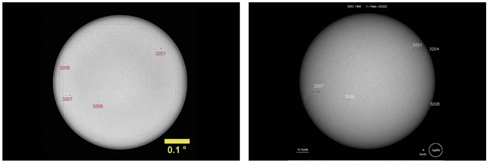
The metalens image on the left, as compared to NASA’s image on the right, with major sun spots annotated. Credit: Capasso Lab, Harvard SEAS
To further explore the applications of their metalens in astronomy, the team subjected the structure to extreme temperatures and temperature changes, similar to what a lens may experience in space. The metalens showed no significant changes after 10 cycles between –195.8°C (liquid nitrogen bath) to 200°C (hot plate). It also showed no significant damage after a vibration stress test, making it a promising choice for launching into space.
As larger wafers become more common in the semiconductor industry—fabrication capacity of 300-mm wafers is expected to expand noticeably by 2025— the tools for creating large-scale metalenses directly may become available. Until then, however, the stitching method developed by the SEAS researchers provides an accessible route for achieving large-scale metalenses.
The researchers also suggest that higher resolution manufacturing techniques, such as deep-ultraviolet immersion lithography, could be used to produce even smaller nanostructures on the metalens.
The paper, published in ACS Nano, is “All-glass 100 mm diameter visible metalens for imaging the cosmos” (DOI: 10.1021/acsnano.3c09462).