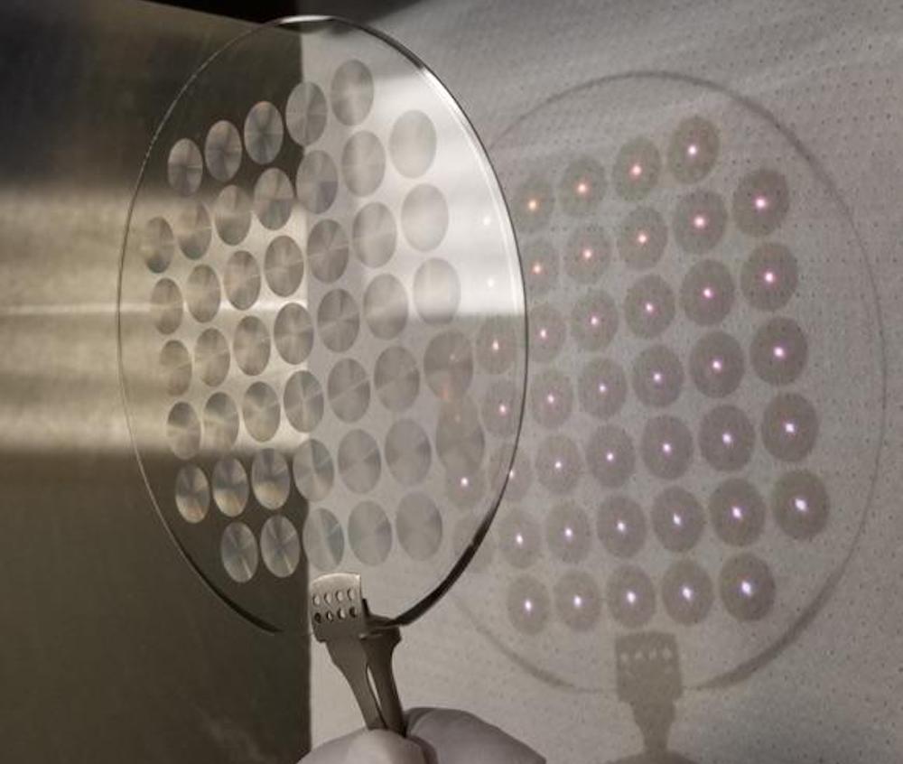
[Image above] A conventional chip fabrication method could be key to mass producing large-scale metalenses. Credit: Joon-Suh Park, Harvard SEAS
What if instead of a camera containing multiple large lenses, you could get the same image quality from a camera using a single lens? That may be possible—if you use a metalens.
Metalenses are flat, engineered lenses constructed of nanoscale arrays of columns or fin-like structures, a design that lets them focus light without causing chromatic aberrations (a type of image distortion that conventionally requires multiple lenses to correct). Researchers at the Harvard School of Engineering and Applied Sciences (SEAS) first demonstrated the efficiency of metalenses in 2016.
I first wrote about metalenses in November 2018. At that time, the Harvard SEAS researchers had developed the first metalens that could focus the entire visible spectrum of light at one time, and a team from the University of Washington and National Tsing Hua University in Taiwan designed a solution to the nanostructure array thickness limitation.
Since then, the Harvard SEAS researchers created a broadband achromatic metalens that focuses light regardless of polarization, and a team of engineers from the University of Pennsylvania made a nanostructured diamond metalens for compact quantum technologies.
As is often the case with academic research, the metalenses used in these studies did not come from a mass-produced stockpile—they were individually created for each study and fairly small in size. However, based on a new paper by the Harvard SEAS researchers, that may soon change.
“Previously, we were not able to achieve mass-production of centimeter-scale metalenses at visible wavelengths because we were either using electron-beam lithography, which is too time consuming, or a technique called i-line stepper lithography, which does not have enough resolution to pattern the required subwavelength-sized structures,” says Joon-Suh Park, a Ph.D. candidate at SEAS and first author of the paper, in a Harvard SEAS press release.
In the new study, the researchers discovered that a conventional chip fabrication method—deep-ultraviolet projection lithography—could solve the production challenge.
“Unlike previous studies which needed a separate deposition process of high-refractive-index dielectric materials … on a transparent substrate to realize a metalens,” they explain in the paper, “here we use low-refractive-index fused silica (SiO2) as both substrate and constituent material to demonstrate a single-material metalens with obvious advantages in terms of mass-production time, simpler fabrication process, and cost.”
Essentially, deep-ultraviolet projection lithography lets the researchers produce many metalenses per chip, each made of millions of nanoscale elements, with a single shot of exposure. This technique not only makes mass production possible but also makes creating larger lens sizes easier. (To date, most lenses are about the size of a piece of glitter; this technique increases size to the centimeter scale.)
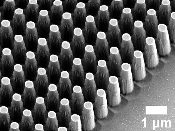
Zoom-in SEM image of nanopillars of the metalens. Credit: Joon-Suh Park, Harvard SEAS
“This research paves the way for so-called wafer level cameras for cell phones, where the CMOS chip and the metalenses can be directly stacked on top of each other with easy optical alignment because they are both flat,” Federico Capasso, senior author of the paper and Robert L. Wallace Professor of Applied Physics and Vinton Hayes Senior Research Fellow in Electrical Engineering at SEAS, says in the press release.
While these mass-produced metalenses are chromatic, meaning all the different colors of light do not focus at the same spot, the researchers are working on creating large-diameter achromatic metalenses.
The paper, published in Nano Letters, is “All-glass, large metalens at visible wavelength using deep-ultraviolet projection lithography” (DOI: 10.1021/acs.nanolett.9b03333).