
[Image above] Optical nanoscopy uses laser beams to strike free electrons, scattering light and providing insights into electron distribution and dynamics within semiconductor materials. Credit: Laser Thermal Lab, UC Berkeley
Since Intel cofounder Gordon Moore predicted in 1965 how integral miniaturization would become to the electronics field, the succeeding decades showed his predictions to be true.
Today, the traditional method for miniaturizing electronics is reaching fundamental limits. But new device structures and materials enable manufacturers to produce even smaller, more powerful semiconductor chips.
To properly test these novel designs, researchers must have techniques capable of measuring phenomena at the picosecond time and nanometer length scales simultaneously.
Time-resolved terahertz spectroscopy, which probes the properties of matter with short pulses of terahertz radiation, has been widely used to study charge carrier dynamics in bulk and nanostructured semiconductors. Its application on the nanoscale has been further developed through integration of scattering-type scanning near-field optical microscopy and pump−probe microscopy.
“However, given the limited photon energy, the efforts have been primarily focused on studying carrier dynamics in narrow bandgap semiconductors, such as InAs and Hg1−xCdxTe, or graphene plasmon,” researchers write in a recent paper.
The researchers are led by the University of California, Berkeley, and include a colleague from Laser Prismatics LLC in California. In their paper, they propose a method that combines ultrafast nanoscale measurements and theoretical modeling to probe carrier behavior in semiconductors with wider bandgaps.
Their optical nanoscopy method integrates near-field scanning optical microscopy and pump-probe optics “to enable high resolution at both spatial and temporal scales,” says Costas Grigoropoulos, senior author and A. Martin Berlin Chair in Mechanical Engineering and Distinguished Professor of Mechanical Engineering at UC Berkeley, in a UC Berkeley press release.
As shown in the schematic below, their setup consists of an 800-nm femtosecond laser beam split by a beam splitter into a probe beam and a pump beam. The pump beam is frequency doubled to 400 nm by a nonlinear crystal (beta barium borate) and then amplitude-modulated by an acoustic-optic modulator.
The probe beam passes through a mechanical delay stage, and then both beams are merged and directed via a parabolic mirror to a platinum-coated atomic force microscope (AFM) tip with an oscillating frequency.
The scattered probe light is collected by the parabolic mirror and redirected to an avalanche photodiode detector (APD), where it is interfered with a reference beam from the reference mirror. A long-pass filter is placed before the detector to block the scattered pump beam.
Finally, the APD signal is sent to a lock-in amplifier for signal demodulation at the same modulation frequency of the pump beam to suppress background noise.
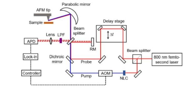
Experimental setup of the new optical nanoscopy system. NLC: nonlinear crystal; AOM: acoustic-optic modulator; APD: avalanche photodiode; LPF: long-pass filter; RM: reference mirror. Reprinted with permission from Li et al., Nano Letters. Copyright 2023 American Chemical Society.
The experimental data validated that the point-dipole model provides a good qualitative description of the carrier behavior.
Based on these findings, the researchers state their method will be useful in analyzing other wider bandgap semiconductors, such as gallium arsenide (bandgap of 1.42 eV).
Additionally, the method “provides a promising tool to study other nonequilibrium thermodynamic phenomena in nanomaterial systems, including phase transitions, energy and charge transfer, and phonon propagation,” they conclude.
The paper, published in Nano Letters, is “Ultrafast optical nanoscopy of carrier dynamics in silicon nanowires” (DOI: 10.1021/acs.nanolett.2c04790).