[Image above] How do you prevent your electronics from burning out? Since their commercial introduction in the 1970s, varistors are the preferred devices for protecting sensitive electronic circuits. Credit: Thermal problem, Flickr (CC BY-NC-SA 2.0)
Smells evoke powerful memories. The sweet odor of chocolate chip cookies baking: good memories. The sweet phenolic smell of electric circuits overheating: not so good.
As armor protects the wearer from weapons, special devices are used to protect electrical circuits from high voltage and high currents. Such devices include fuses, circuit breakers, and metal oxide variable resistors (MOVs).
MOVs, also called varistors, are the preferred devices for sensitive electronic circuits since their commercial introduction in the 1970s. At low applied voltages, varistors are highly resistive ohmic elements, meaning little to no current flows through them. But once the threshold voltage, also known as clamping voltage or breakdown voltage, is exceeded, the varistor switches to a highly conductive element that allows the current to bypass the sensitive electronics, much like a spillway siphons off excess water from a dam in high-water conditions. Once the voltage drops below the threshold voltage level, the varistor returns to the resistive state.
This switching ability provides two distinct advantages over fuses or circuit breakers:
- The circuit continues to run even under nonideal conditions.
- No manual intervention is required to reset the system.
Even though MOV technology is over 40 years old, research still is actively conducted today to improve both production and performance.
Performance criteria for varistors
MOVs are typically composed of zinc oxide doped with bismuth, cobalt, manganese and other functional metal oxides. As with most ceramic devices, manufacturers seek to decrease production temperatures and cycle times to use less fuel and lower-cost electrical contact materials while increasing production rates. Sintering temperatures up to 1,250˚C require expensive contact materials such as palladium. Reducing the sintering temperature to below 950˚C enables the use of silver instead.
Recent papers published in the ACerS journals International Journal of Applied Ceramic Technology (ACT) and International Journal of Ceramic Engineering and Science (IJCES) detail experiments aimed at improving processing through use of additives, nanoscale materials, and advanced sintering techniques. These journals also include studies on improving performance of varistors.
Fortunately, the major performance criteria for varistors are readily described and measured using voltage-current experiments. One such graph using data from the open-access paper “Superior performing nano‐enabled metal oxide varistors” published in IJCES is shown below.
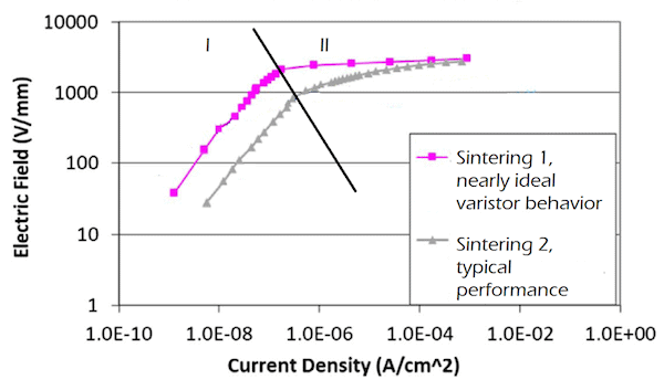
Region I is the ohmic resistor region. The higher the ohmic resistance, the lower the leakage current (current going through the resistor at voltages less than breakdown level). High leakage currents waste energy, leading to additional heat and shorter battery lives. The nearly ideal varistor shows nearly ten-fold lower leakage currents than seen in the typical performing varistors.
Region II is the conduction or voltage clamping region. The lower the slope in this region, the quicker the response of the varistor to over-voltages. The slope, or more correctly the inverse of the slope, defines the nonlinearity coefficient α. Higher α means better response time and better protection since the over-voltage drift is minimal.
The other parameter in region II is the absolute value of the clamping voltage. For a given composition, the clamping voltage is inversely proportional to the grain size. In other words, larger grains lead to lower clamping voltage. The behavior of varistors is dependent on the thickness, composition, and quantity of grain boundaries in a given volume. And while large grains lead to a lower number of grain boundaries and therefore lower clamping voltage, variations in grain size distribution and density/porosity of the ceramic lead to variations in the leakage current and alpha coefficient.
Advances in varistor processing and performance
In the article “Low-temperature sintering and electrical properties of BBSZ glass-doped ZnO-based multilayer varistors,” the researchers, lead by Yuanxun Li from the University of Electronic Science and Technology of China, explored the effects of adding a glass composed of bismuth, boron, silicon, and zinc oxides on the sintering of a multilayer MOV device. The glass enhances liquid phase sintering. The researchers achieved high-density ceramics at temperatures below 950˚C. They achieved the best results at 3% glass load fired at 925˚C, with their lowest leakage currents and α values above 40, which is comparable to commercial device performance.
In the article “Superior performing nano‐enabled metal oxide varistors,” Daniel Tan from Guangdong Technion Israel Institute of Technology focused on using nanoscale powders while exploring advanced sintering techniques. His work resulted in finer grains (from less than 1 to 3 micrometer versus 7–15 micrometers for commercial powders) and thus higher values of breakdown voltages. Using traditional air-atmosphere unconstrained sintering, nanoscale materials sintered at 1,050˚C showed performance comparable to commercial MOV materials sintered at 1,200˚C. Adding additional bismuth oxide to enhance liquid-phase sintering greatly improved alpha (to nearly 80) but decreased the clamping voltage, the latter of which is attributed to higher number of grain boundaries per unit volume.
Using microwave-enhanced sintering, Tan did not see substantial improvements to the sintering cycle or performance of the MOV. However, the results from spark plasma sintering (SPS) are both interesting and complicated. Oxygen scarcity during SPS was a significant factor. Tan overcame oxygen scarcity through partial sintering via SPS and a second sintering in air. The best performance was achieved though second-stage sintering at 950˚C, with very high clamping voltage, very low leakage currents, and α around 50.
For more information on these improvements, read the full articles at the links below.
“Low-temperature sintering and electrical properties of BBSZ glass-doped ZnO-based multilayer varistors,” available online now (DOI: 10.1111/ijac.13367) and soon to be released in a special issue of the International Journal of Applied Ceramic Technology highlighting work presented at the 2019 International Conference and Exhibition on Ceramic Interconnect and Ceramic Microsystems Technologies (CIMCT-2019).
“Superior performing nano‐enabled metal oxide varistors,” published open-access in International Journal of Ceramic Engineering and Science (DOI: 10.1002/ces2.10017).