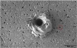

A representative “puncture” caused by dielectric breakdown of the alumina. A surface pit formed by grain pull-out is circled red, although there are clearly many. Credit: Shetty, et al; Wiley.
If you expect something to break, there are two things you want to know—when and how bad. Anyone who has broken a bone, for example, knows there is a big difference between a stress fracture and a compound fracture. Curious minds, however, also want to know why. The idea is to anticipate and control failure.
These motivations lie at the heart of testing. In its essence, testing comes down to isolating variables or effects and accurately interpreting the results. A new paper in the Journal of the American Ceramic Society appears at first glance to offer a new way of evaluating dielectric properties of alumina, but there is more to this story.
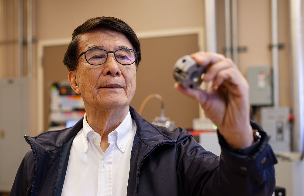
The paper, “Dielectric Breakdown of Polycrystalline Alumina: A Weakest-Link Failure Analysis,” reports on research by a group led by Dinesh Shetty, professor of materials science and engineering at the University of Utah. Alumina serves as an insulator in a wide range of applications from mundane spark plugs to sophisticated medical instrumentation. It is not good when its dielectric strength is exceeded and it fails.
A key challenge to measuring dielectric strength is that external factors, such as specimen configuration and variations in such microstructural features as grain size and porosity, can exert more influence than the intrinsic properties. Standardized tests for measuring dielectric strength do not account for variations in field intensity with extrinsic factors. For example, when dielectric strength is measured with flat electrodes against a flat sample as specified by ASTM standard D149-97a, the electric field is most intense at the edges.
Shetty’s team looked at a variety of extrinsic factors and their influence on dielectric strength. Extrinsic factors included electrode geometry and size, dielectric constant of the dielectric oil, and specimen thickness. To evaluate their results, the group took advantage of Shetty’s expertise with finite element analysis and weakest link theory—tools that are typically associated with mechanical property analysis.
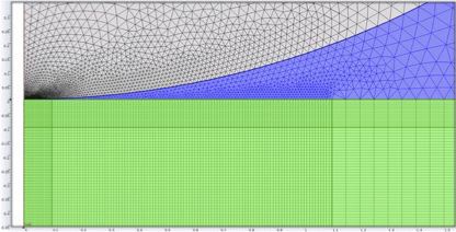
These tools allowed the team to investigate the effects of electric field variations. “We were the first to do a careful analysis of electric field distribution and use local electric field to describe dielectric breakdown,” Shetty said in a phone interview regarding applying finite element analysis to electrical fields. The image above shows the finite mesh used to calculate electric fields in polycrystalline alumina (green) with spherical electrodes (white) and a dielectric liquid (blue). The liquid, an oil, prevents arcing and forces the system to find its breakdown pathway in the ceramic (Credit: Shetty, et al, Wiley.)
Using a ball-and-ring electrode configuration, the researchers noticed that the breakdown field scales with electrode size and is higher when the electrical field is localized, for example, in thin samples tested with small ball electrodes. This trend was familiar to Shetty. “This scaling effect of the electrically stressed ceramic surface area or volume suggested that dielectric breakdown of alumina might be exhibiting the characteristics of a weakest-link failure phenomenon analogous to brittle fracture,” he writes in the paper, which also explains that “weakest-link failure” is the “theory of extreme values,” and describes the “mathematical relationship between a population distribution and the distribution of the lowest values” in a sampling of the population.
The team considered two defect distribution paradigms to describe the FEA results—the familiar Weibull distribution and the Laplace distribution. The Laplace distribution fit the data closely; the Weibull distribution did not. This was an important discovery, because the Laplace distribution describes surface defect distributions, not bulk defect distributions. Initially, Shetty said he expected that the weakest-link flaws would be in the bulk, but the FEA and its fit with the Laplace distribution showed that the fatal flaws were on the surface. In fact, flaws more than 100 µm below the surface do not matter.
Realizing the importance of surface defects, the team also noticed pits on the surface of their alumina samples that were about the same size as the grains. Suspecting grain pull-out during finishing, they carefully repolished the samples to minimize grain pull-out and measured again. Tests confirmed that dielectric strength correlates directly with surface pit density—that is, the samples with better surface finishes had higher dielectric strengths.
Shetty thinks this approach to measuring dielectric strength would work for other materials, too. It is interesting to note that an electrical measurement provided information about processing effects, which could have quality control applications.
Author
Eileen De Guire
CTT Categories
- Basic Science
- Electronics


