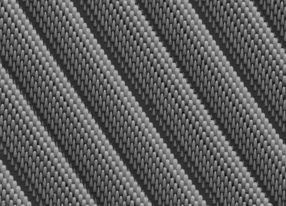
[Image above] Could nanofocused, graphene-based mid-infrared sensors improve nanometric molecular analysis? Credit: Daria Sokol, MIPT Press Office
One topic that has caught my eye recently is infrared radiation (IR).
IR is the wavelength region between visible light and microwaves, roughly 700 nanometers to 1 millimeter. All objects emit and absorb IR to some extent, which makes sensors that detect IR invaluable to science—from investigating chemical compositions and reactions to detecting planets and diagnosing diseases.
Improving IR detectors is an active area of research. And in May, I wrote about a proposed graphene-based detector that might expand the spectral operating range of quantum-based photodetectors. Today, I look at another study that proposes using graphene to improve IR detectors.
Molecular analysis via mid-IR spectroscopy
Mid-IR spectroscopy is an important tool for both organic and inorganic chemists because the technique allows them to nondestructively analyze molecules.
It works by illuminating a sample with incident IR light, some of which is absorbed. A detector then captures the transmitted or reflected light, and it uses this information to deduce what molecules the sample is made of based on what IR frequencies the sample absorbed.
Mid-IR spectroscopy runs into a problem, though, when used to study small amounts of molecules in nanometric volumes.
“… the cross-section of the [sample] is much smaller than the wavelength of light, and thus the absorption or scattering signals are too small to be detected,” researchers write in a recent open-access paper.
The researchers, from several institutions in Spain and the Moscow Institute of Physics and Technology (MIPT) in Russia, explain this difficulty can be partially overcome by exciting surface plasmon polaritons (SPPs) on the surface of a conductor.
SPPs are a type of surface wave that exist at the interface between a conductive material, such as metal, and a dielectric material, such as air. The waves consist of free electrons in the conductive material (surface plasmons) coupled with electromagnetic waves in the dielectric material. The coupled electromagnetic waves–electrons are called polaritons, and they propagate together along the conductive–dielectric interface.
SPPs are shorter in wavelength than the incident light, so harnessing SPPs to analyze a sample improves absorption and scattering signals on the sample’s small cross-section. And graphene in particular supports SPPs with shorter wavelengths.
“Unlike metals, graphene supports plasmon polaritons with much larger wavevectors, and as a consequence, much stronger vertical field confinement,” the researchers write in the paper.
(A wavevector describes how a wave propagates through a medium. Its wavenumber, or the number of oscillations per length unit, is inversely proportional to wavelength, so a larger wavevector means a smaller wavelength.)
However, even though the wavelengths of SPPs in graphene are shorter, “we can’t get the cross-section area smaller than the diffraction limit using the standard focusing technique,” Kirill Voronin, paper co-author and graduate student in the Laboratory of Nanooptics and Plasmonics at MIPT, explains in an email. In other words, the waves were still too long to be properly absorbed and scattered by a nanometric sample.
To shorten the SPP wavelength even further, the researchers decided to investigate nanofocusing.
Nanofocusing: A technique for analyzing the nanoworld
In nanofocusing, light is sent along a tapered waveguide so that both its cross-section and wavelength gradually reduce, leading to a dramatic increase of the electromagnetic field intensity at the taper apex.
Some studies, such as this one, reported the possibility of using nanofocusing to shorten the wavelength of graphene-based SPPs, but the technique’s “application for molecular sensing has not yet been explored,” the researchers write.
Nanofocused graphene SPPs enhance mid-IR molecular analysis
To explore use of nanofocused graphene SPPs for molecular sensing, the researchers designed a wedge-shaped structure consisting of two sides made from graphene and conductive metal, with a tapering layer of dielectric material filling the space in between.

Schematic of the wedge-shaped nanofocusing structure. Credit: Voronin et al., Nanophotonics (CC BY 4.0)
Through simulation, the researchers placed a layer of CBP, a molecule used in pharmaceutics and organic light emitting diodes, between the metal and graphene sides. Compared to an analysis using graphene without the nanofocusing setup, nanofocusing resulted in much better resolution.

The reflection coefficient of graphene plasmons without (a,b) and with (c,d) nanofocusing. The reflection coefficient depends on frequency, and the maximum frequency coincides with the molecules’ absorption peak. The reflection coefficient is tens of percent lower for the nanofocused sampling, meaning radiation is being strongly absorbed. Credit: Voronin et al., Nanophotonics (CC BY 4.0)
In the conclusion, the researchers note their design could be used for creating actual devices after certain improvements to the technological processes are resolved. In addition, “other 2D materials can also be potentially used for polaritonic focusing and sensing based on the same principles here reported,” they write.
The open-access paper, published in Nanophotonics, is “Nanofocusing of acoustic graphene plasmon polaritons for enhancing mid-infrared molecular fingerprints” (DOI: 10.1515/nanoph-2020-0164).
Author
Lisa McDonald
CTT Categories
- Modeling & Simulation
- Nanomaterials


