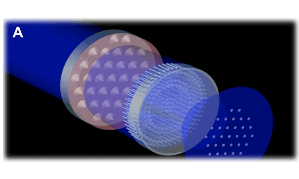
[Image above] Schematic of patterned sapphire substrates inspected by the metalens. Credit: Chen et al., Scientific Reports (CC BY 4.0)
In the not-too-distant future, cameras may no longer need multiple different lenses to focus an image—a single metalens would do the trick.
Metalenses are flat, engineered lenses constructed of nanoscale arrays of columns or fin-like structures. Because of their design, metalenses focus light without causing chromatic aberrations, a type of image distortion that conventionally requires multiple curved lenses to correct.
Researchers at the Harvard School of Engineering and Applied Sciences (SEAS) conducted much of the foundational research on metalenses, starting with the first demonstration of metalens efficiency in 2016. We’ve covered several of the advances since then, including development of metalenses that focus the entire spectrum of visible light and a technique to mass produce metalenses.
This year, metalenses are just starting to move toward commercial development. However, much research still needs to be done to make this material a mainstay of next-generation imaging and illumination technologies. Fortunately, many research groups outside of Harvard SEAS have taken an interest in metalenses as well, such as a Taiwan-based group that just published an open-access paper in Scientific Reports.
The Taiwan group includes researchers from National Taiwan University in Taipei and National United University in Miaoli. In their study, they looked to develop a metalens to serve a very specific purpose—as a replacement for traditional imaging technologies used to examine the substrate on which gallium nitride-based blue light-emitting diodes (LEDs) are grown.
Gallium nitride is a wide bandgap semiconductor that revolutionized development of white and blue LEDs in the 1990s. Gallium nitride is still the material used in many LEDs today, and researchers expect gallium nitride to play an important role in next-generation high-power electronics, high-frequency devices, and laser diodes as well.
Gallium nitride-based blue LEDs are typically grown on micro/nano-sized patterned sapphire substrates (PSSs) to improve light extraction efficiency of the final LED. PSSs are examined using a scanning electron microscope (SEM) or optical microscope to ensure the substrate has the correct structure. However, SEM systems can be costly and slow, while optical microscopes are bulky and complex devices.
Thus, “There is a need to develop ultra-light and thin optics to replace current conventional objectives,” the researchers write.
They note that highly efficient metalenses were recently constructed with a Pancharatnam-Berry phase rotational morphology, but these metalenses required circularly polarized light as an excitation incidence to reach their full-phase control.
“Although this obstacle can be circumvented by using nanostructures with symmetric cross-sections, polarization-insensitive metalenses of high performance for the desired wavelength require the development of highly efficient building blocks along with carefully selected subwavelength periods and well-established fabrication processes,” they write.
They decided to develop metalenses using high-aspect-ratio gallium nitride hexagon-resonated elements as the building blocks. (High-aspect-ratio nanostructures have a length many times that of their width.) Using a metal–organic chemical vapor deposition system and electron-beam lithography, they fabricated three metalenses that work at three distinct wavelengths of 405, 532, and 633 nm, with respective diffraction-limited focusing efficiencies of 93%, 86%, and 92%.
Testing revealed the 405-nm metalens capable of taking “exceptional clear” images of line features, with the smallest resolvable features having widths of 870 nm. In contrast, line features in images formed by the 532-nm metalens lost clarity when approaching line widths of 0.98 μm, while the 633-nm metalens blurred due to the larger diffraction-limited value of the metalens.
The researchers fabricated another metalens working at the wavelength of 450 nm and compared its imaging capabilities to an SEM. “Unsurprisingly, the one taken by the [SEM] shown in Fig. 5J, is vaguer than the image pictured by the 450-nm-designed metalens, as verified in Fig. 5K, which can clearly and sharply visualize the post apexes in the PSS,” they write.

Images of the PSS on which the blue LED is grown. Images taken by (J) SEM (numerical aperture = 0.4) at the laser wavelength of 450 nm, and (K) the 450-nm-designed metalens (numerical aperture = 0.3) at the laser wavelength of 450 nm. Scale bar: 3 μm. Credit: Chen et al., Scientific Reports (CC BY 4.0)
The researchers conclude that “This work demonstrates the tremendous capacity for the ultra-thin and light-weight metalenses being used for fabricated structure inspection of the patterned substrates and offers another novel and advanced optics based on semiconductor manufacturing.”
The open-access paper, published in Scientific Reports, is “Polarization-insensitive GaN metalenses at visible wavelengths” (DOI: 10.1038/s41598-021-94176-7).