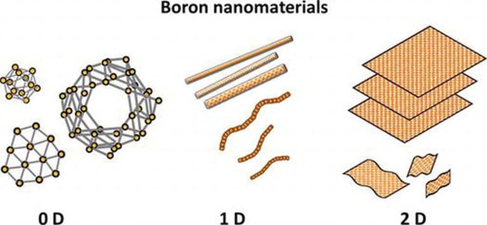
[Image above] Illustration of various types of zero, one, and two-dimensional boron nanomaterials, such as nanoclusters, nanowires, nanotubes, nanobelts, nanoribbons, and nanosheets. Credit: Kondo, Science and Technology of Advanced Materials (CC BY 4.0)
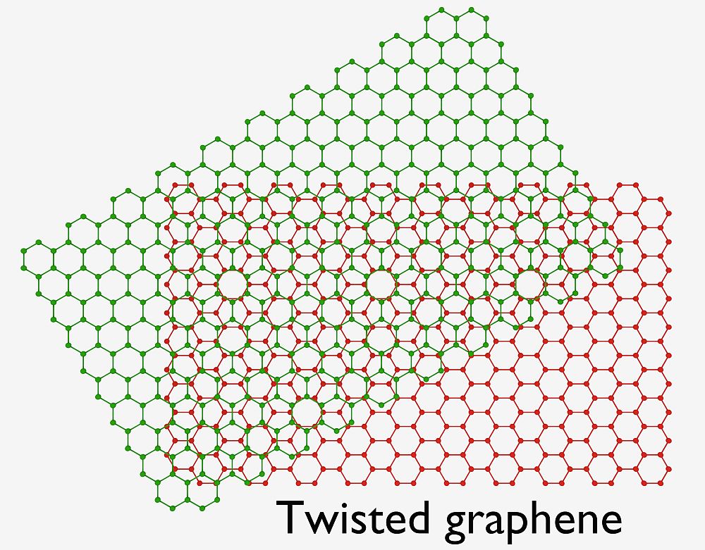
In the world of 2D nanomaterials, carbon nanostructures are unique in that many other advanced nanosystems are multielement compounds (e.g., hexagonal boron nitride, MXenes).
Carbon naturally forms in flat, layered structures when bonding with itself, which allows for easy development of free-standing, long-lasting sheets. In contrast, other single element systems, such as silicene (2D silicon) and phosphorene (2D phosphorous), prefer to bond in buckled or corrugated shapes, which is not conducive to stable sheet development.
What these single element systems lack in mechanical stability, however, is made up for in other ways. Boron, for example, features a unique electron-deficient nature that allows it to assume numerous complex structural configurations. As such, boron offers much greater structural mobility than carbon, which researchers expect will streamline its adaptation into different devices and applications.
(While realizing more planar structures with boron is possible, it often leads to dangling bonds that make 2D boron prone to rapid oxidization in air. On the other hand, researchers have shown that forming lattices consisting of multiple structural configurations can lead to very stable nanomaterials.)
Like carbon nanomaterials, boron nanomaterials are typically formed through methods such as chemical vapor deposition, arc-discharge synthesis, and ball milling. However, in the past decade, computational exploration of boron nanomaterials has dominated over experimental studies, meaning such materials are still far away from commercial introduction.
In an open-access paper published last week, an international group of researchers made a new addition to the experimental literature. Led by the University of KwaZulu-Natal in South Africa, the researchers demonstrated that a technique they previously employed to synthesize molybdenum disulfide nanorods—double-pulse laser ablation—can be used to synthesize boron nanomaterials as well.
Laser ablation is a type of physical vapor deposition. In this method, a laser beam is used to vaporize (ablate) the surface of a solid target material. The resulting atoms and clusters, energized by photons in the laser pulse, form a plasma plume that expands outwards and deposits the nanoparticles on a substrate.

General schematic of nanoparticle generation through laser ablation. Credit: Kim et al., KONA Powder and Particle Journal (CC BY 4.0)
It is difficult to control size distribution, agglomeration, and crystal structure in the conventional laser ablation process. Fortunately, advanced laser ablation techniques, such as double-pulse laser ablation, can improve morphology control.
In the new study, the researchers used laser pulses with 1064 and 532 nm wavelengths, operating at a 10 Hz pulse repetition rate. Argon gas was used to slow expansion of the laser-ablated plume and help carry the as-formed nanomaterials to the rear of the quartz tube in which the experiment took place.
Thermodynamic conditions influenced the type of boron nanostructure that formed, with experiments conducted at 800°C, 900°C, and 1,000°C forming boron nanorods, boron nanowires, and bamboo-like boron nanotubes, respectively.
Analysis of the rod, wire, and tube morphologies revealed structures with lateral diameters between 10–100 nm and with lengths ranging from 0.2–1.5 μm. Each nanostructure exhibited improved electrical and optical properties over the source bulk boron.
The results demonstrate that “The laser ablation technique, when combined with a high temperature tube furnace, is a unique method to produce novel nanomaterials,” the researchers conclude.
The open-access paper, published in physica status solidi (a) – applications and materials science, is “High temperature laser assisted synthesis of boron nanorods, nanowires and bamboo-like nanotubes” (DOI: 10.1002/pssa.202200464).