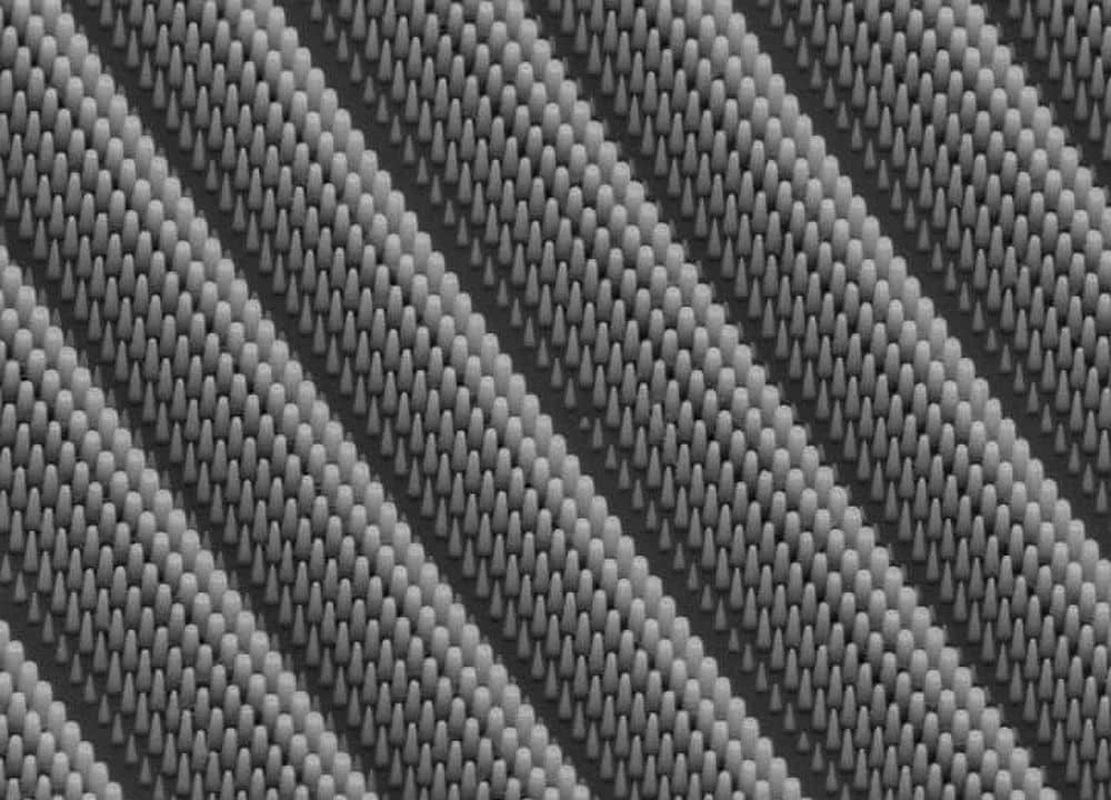
[Image above] Researchers at École Polytechnique Fédérale de Lausanne developed a high-precision nanolithography method that enables them to carve nanometric patterns into 2D materials. Credit: EPFL
“Why cannot we write the entire 24 volumes of the Encyclopedia Britannica on the head of a pin?”
When Richard Feynman posed this question during his lecture at the American Physical Society annual meeting in 1959, he may not have realized his vision of designing on the microscale would prove so prescient. But 60 years later, nanoscience and nanotechnology is a huge area of research, one that we regularly cover on CTT.
Since the turn of the century, scientists have expanded beyond just creating nanomaterials to perfecting methods that allow design of specific nanostructures. These methods can be categorized into two groups: top-down techniques, which involve etching away bulk material to achieve small structural architectures; and bottom-up techniques, which involve building structures atom-by-atom or molecule-by-molecule.
To date, top-down approaches to nanostructure construction are used extensively in the semiconductor industry to fabricate integrated circuits, among other things. Specifically, lithographic techniques—or techniques by which a pattern is transferred onto a surface—are typically used.
Common lithographic techniques involve using beams of light, electrons, or ions to etch patterns onto a surface. However, though these techniques work well for fabricating nanostructures on most surfaces, they run into some challenges when used to pattern 2D materials. For example, this study observed structural damage when particles struck the 2D surface.
Many 2D materials are semiconductors, and so they are of great interest for the electronics industry. Thus, alternative lithographic techniques are needed to effectively fabricate nanostructures in 2D materials.
Scanning probe lithography (SPL) is one type of lithography that holds potential for this purpose. Instead of using a focused beam of particles to etch patterns in a sample, SPL methods use a physical tip to modify the surface through various physical and chemical interactions, such as scratching, nanoindentation, or heating.
Among SPL methods, thermal scanning probe lithography (t‐SPL) has gained much attention in recent years. This method involves using a heated nanotip to modify the surface of a sample, and it has now reached a high level of technical maturity, with several dedicated tools to perform reliable t-SPL.
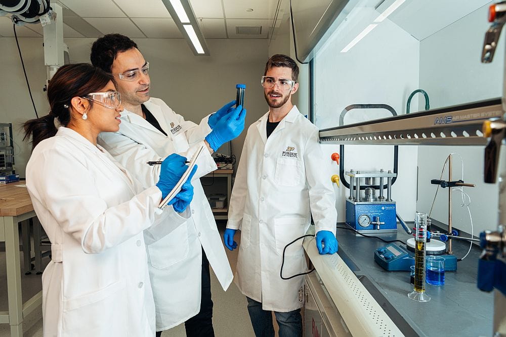
In a recent open-access study, researchers at École Polytechnique Fédérale de Lausanne (EPFL) in Switzerland explored using t-SPL to fabricate nanostructures in 2D materials. Compared to previous SPL studies that relied mainly on mechanical scratching to cut patterns, they made a significant change to the setup of their experiment to fully harness the thermal component of t-SPL.
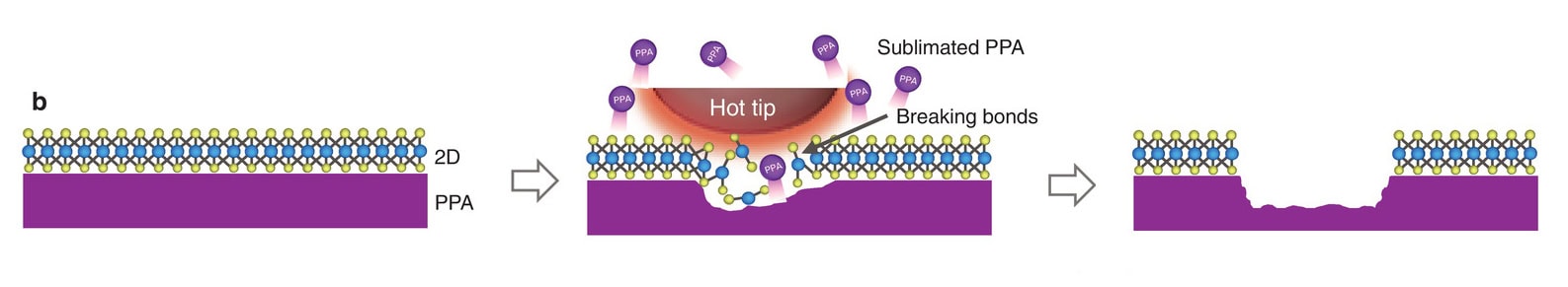
Instead of placing the 2D materials directly on an inelastic substrate, they placed a polymer layer between the 2D layer and substrate. “The polymer we use is polyphthalaldehyde (PPA) with a glass transition temperature of ≈150°C. Above this temperature, … PPA does not melt but directly sublimates,” they write in the paper.
When they pressed the heated tip into the 2D material, sublimation of the underlying polymer layer allowed the tip to achieve a deeper indention, thus making it easier to cut through the 2D material’s chemical bonds.
The researchers used the t-SPL method to create square patterns in a variety of molybdenum-based 2D materials, with pattern sizes ranging from 20 to 200 nm. “The smallest feature we were able to cut is about 20 nm, which is the smallest reported for a direct cutting method and is similar to the resolution in [electron beam lithography],” they write.
They also note their method is not limited to cutting monolayers but also can be used to cut certain multilayers and, “most interestingly,” heterostructures. They acknowledge graphene, even at monolayer thickness, could not be fractured “as the intra‐layer bonding exceeds the force that can be applied with the t‐SPL tool,” but they say this limitation “could be eventually overcome with a t‐SPL cantilever that can apply larger contact forces.”
In an EPFL press release, first author Xia Liu, researcher and postdoc in the School of Engineering’s Microsystems Laboratory, says their technique could prove quite useful to the semiconductor industry.
“This generic technology will be very useful in nanoelectronics, nanophotonics, and nanobiotechnology, as it will help to make electronic components smaller and more efficient,” she says.
The open-access paper, published in Advanced Materials, is “Thermomechanical nanocutting of 2D materials” (DOI: 10.1002/adma.202001232).