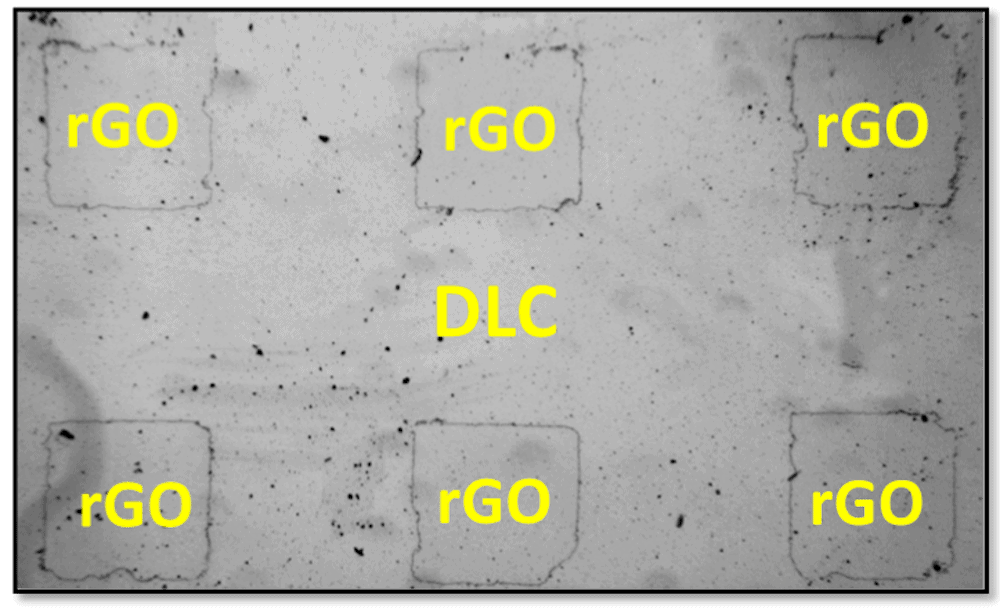
[Image above] Optical image of laser-patterned reduced graphene oxide (rGO) blocks on diamond-like carbon (DLC) films deposited on a silicon (100) substrate. Credit: Reprinted with permission from ACS Appl. Mater. Interfaces 2019, 11, 2724318–24330. Copyright 2019 American Chemical Society.
Not only is carbon the basis of all organic life, it is also the basis for many advanced technologies. For example, carbon fiber supports the structure of many planes, cars, and boats; diamonds are the linchpin to certain semiconductors, magnetometers, and lasers; and graphene shows high potential to transform countless industries.
Creating these carbon-based materials, however, is difficult, which can lead to poor-quality materials that hinder research. So developing simpler techniques to create high-quality carbon-based materials are needed.
North Carolina State University researchers led by Jagdish (Jay) Narayan, chair professor in the materials science and engineering department, have made progress on this front using pulsed laser annealing (PLA).
PLA involves melting materials using a highly energetic spatially and temporally confined laser pulse. PLA is a nonequilibrium processing technique, meaning the materials being processed are not in thermodynamic equilibrium. “Such processing allows us to develop new materials which are very difficult to fabricate with equilibrium-based methods,” Siddharth Gupta, NC State Ph.D. candidate, says in an email.
Narayan’s first article on PLA processing, exploring the creation of continuous diamond films, was published in 1991. “The research group has followed it up with discovery of Q-carbon [here and here] and formation of diamonds in ambient conditions,” Gupta adds.
In a new article published this June, Narayan and Gupta showed PLA can be used to create yet another type of carbon-based material—reduced graphene oxide (rGO).
rGO is a derivative of graphene that solves a challenge inherent to regular graphene: its zero-gap semimetal nature. The zero-gap nature results in an extremely short carrier lifetime, which limits graphene’s applications in the semiconductor industry. In contrast, rGO has a distinct bandgap and high carrier density, which makes it useful as a semiconductor.
In both a 2015 diamond study and these recent rGO experiments, NC State researchers used high-power nanosecond laser pulses to melt carbon and then undercooled the liquid carbon, directing its solidification into either diamond nanostructures or rGO. Gupta says undercooling is the key to determine which structure the liquid carbon solidifies into.
“In PLA processing, substrate plays a major role in determining the undercooling of carbon melt,” he explains. The 2015 diamond study used substrates of sapphire, plastic, and glass. The rGO study used a silicon substrate.
“In the case of silicon, due to the higher thermal conductivity, most of the heat flux leaks through the substrate, significantly limiting the undercooling,” Gupta explains. “Under such low undercooling conditions and short melt lifetimes in controlled environment, we achieved the formation of highly reduced graphene oxide.”
(There is an exception to the substrate’s major role. A study published this January by Narayan’s group shows carbon nanofibers and nanotubes, in contrast to carbon films, provide sufficient undercooling on their own and so could be placed on any substrate for conversion into diamond.)
In an NC State press release, Narayan gives some details on p–n junction diodes the researchers created using the rGO. “The graphene devices are operational at room temperature with charge carrier concentration of −1.2 × 10²¹/cm3 and localization length of 3 nm. The p–n junction heterojunction diodes have a turn-on voltage of 0.3 V, rectification ratio of 110@±1.5 V, and activation energy of 0.13 eV under reverse bias,” he says.

rGO is a promising material for electrochemical sensors and associated applications—PLA offers a simple way to produce the material. Credit: Reprinted with permission from ACS Applied Material Interfaces 2019, 11, 2724318–24330. Copyright 2019 American Chemical Society.
In comparison, to achieve rGO with such characteristics using equilibrium-based methods, films have to be thermally reduced above 2,000 K for more than an hour.
Gupta says they are now working on developing ultrathin CMOS sensors and DRAM devices using PLA. He sees PLA playing a major role in creating graphene-related materials in the future.
“One of the key advantages of PLA processing is that it keeps the rest of the wafer at near-ambient conditions,” he says. “This makes post processing of devices possible, presenting a new use case for graphene-related materials.
The paper, published in ACS Applied Materials & Interfaces, is “Reduced graphene oxide/amorphous carbon p–n junctions: Nanosecond laser patterning” (DOI: 10.1021/acsami.9b05374).
Author
Lisa McDonald
CTT Categories
- Nanomaterials


