[Image above] Synthesizing graphene nanoribbons is a costly and low-yield process by conventional methods. An alternative method developed by researchers in Russia offers higher yield at lower cost. Credit: MIPT Press Office
If I had to choose a favorite element, carbon would definitely make my top five. I find it amazing that this one element, depending on how you arrange the atoms, can demonstrate vastly different properties, from being either very soft (graphite) or extremely hard (diamond) to being either semiconductive (graphene) or conductive (carbon nanotubes).
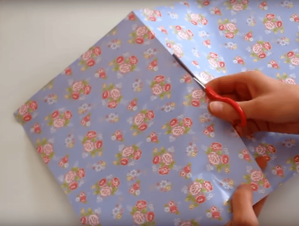
Out of all carbon allotropes, graphene nanoribbons are one family that does not receive as much attention. Graphene nanoribbons are finite strips of graphene with width less than 50 nm. To help with visualization, you can imagine graphene as a roll of honeycomb-shaped wrapping paper, and graphene nanoribbons are the strips that you cut from it.
When you cut wrapping paper, each strip can have a different design along the edge depending on where you cut through the paper. The same concept applies to graphene nanoribbons—the edge geometry of the nanoribbon depends on how you cut the graphene’s honeycomb lattice.

Much like strips of wrapping paper, graphene nanoribbons have different edge geometries depending on how you cut through the graphene’s honeycomb lattice. Credit: cozyandwarm, YouTube
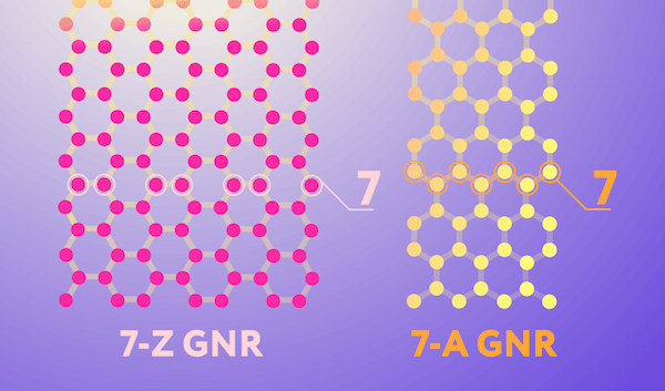
The two most common edge geometries of graphene nanoribbons—zigzag and armchair—are illustrated in the image below. These geometries impart the nanoribbon with noticeably different electronic properties. The zigzag geometry, in which atoms along the edge come from the same sublattice, give the nanoribbon conducting properties. The armchair geometry, in which atoms along the edge come from two different sublattices, give the nanoribbon semiconducting properties that are valuable for electronics.

Two nanoribbon edge configurations. The pink network of carbon atoms is a ribbon with zigzag (Z) edges, and the yellow one has so-called armchair (A) edges. Note that while nanoribbons come in many different widths, the ones in the image are by convention both considered to be seven atoms wide. Credit: Daria Sokol, MIPT Press Office
While the analogy of wrapping paper is useful for visualizing why graphene nanoribbons have different edge geometries, the truth is graphene nanoribbons typically are not created by cutting up graphene sheets or other top-down fabrication methods. Instead, a bottom-up synthesis approach is used because it provides more control over the edge geometry, and it more easily allows production of nanoribbons with narrow widths on the order of a few nanometers.
Bottom-up synthesis of graphene nanoribbons commonly involves on-surface chemical reactions that occur in two stages. In the first stage, halogen-containing molecules are adsorbed on a gold substrate, at which point substrate-assisted dehalogenation and aryl−aryl coupling of monomers into polymeric structures occurs. In the second stage, the polymeric structures are thermally transformed into graphene nanoribbons via cyclodehydrogenation and planarization.
There are several drawbacks to this synthesis process. For one, the process is quite costly due to the gold substrate and the ultrahigh vacuum conditions needed to facilitate efficient aryl−aryl coupling (<10-9 mbar). In addition, very few nanoribbons are produced at a time, so material output is comparatively low for the price.
Fortunately, recent advances in chemical vapor deposition techniques have opened the door to address some of these drawbacks. And researchers led by the Moscow Institute of Physics and Technology (MIPT) in Russia embraced that opportunity in their recent paper, which describes an alternative synthesis method for graphene nanoribbons.
The MIPT researchers, as well as colleagues from Skolkovo Institute of Science and Technology and the A.M. Prokhorov General Physics Institute of the Russian Academy of Sciences, developed the approach based on their previous work growing graphene nanoribbons inside single-walled carbon nanotubes, which served to constrain ribbon width.
“To form surface assisted bottom-up graphene nanoribbons, we used the same setup with modified synthesis parameters and a different substrate and precursor molecules,” say Elena Obraztsova and Pavel Fedotov, head and senior researcher, respectively, at the MIPT Laboratory of Nanocarbon Materials, in an email.
Instead of a gold substrate, they placed a common nickel foil in a glass tube together with a solid precursor (10,10′-dibromo-9,9′-bianthracene molecules, or DBBA). They sealed the tube under moderate vacuum conditions (10-3 mbar) and then placed it in a quartz tube reactor, where it was subjected to the two-stage annealing process.
Multiwavelength Raman spectroscopy testing revealed the graphene nanoribbons produced using the new method compared in quality to graphene nanoribbons fabricated using conventional methods that require ultrahigh vacuum conditions and a gold substrate.
In addition, the nanoribbons grew as thick films that could be separated into multiple ribbons, in contrast to the thin films produced by conventional ultrahigh vacuum processes. Obraztsova and Fedotov say this difference in film thickness is because they optimized the setup to produce thick films rather than monolayers. For example, instead of a careful dose of DBBA molecules used in conventional setups, their process requires DBBA molecules in excess.
The researchers now are working on optimizing the synthesis parameters to produce not only seven-atom armchair graphene nanoribbons but also graphene nanoribbons of different types, by using other molecules besides DBBA.
“In our future studies, we are planning to examine the optical properties of different types of semiconducting graphene nanoribbons,” Obraztsova and Fedotov say. “Our goal is to register characteristic Raman, UV-Vis-IR optical absorption, and photoluminescence that are fingerprints of particular type of graphene nanoribbons.”
The paper, published in The Journal of Physical Chemistry C, is “Excitonic photoluminescence of ultra-narrow 7-armchair graphene nanoribbons grown by a new ‘bottom-up’ approach on a Ni substrate under low vacuum” (DOI: 10.1021/acs.jpcc.0c07369).
Author
Lisa McDonald
CTT Categories
- Electronics
- Nanomaterials


