Last August I wrote about the typical 50% waste created when wire saws are used to slice silicon ingots into PV-suitable wafers, and research being conducted in Germany to lower that waste.
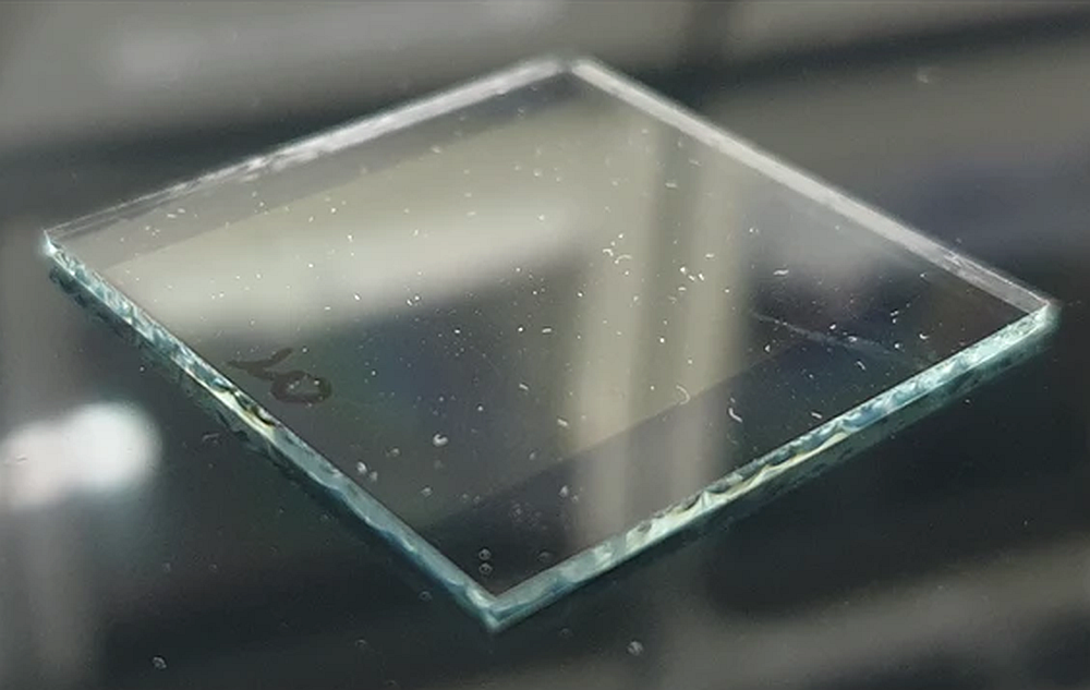
Now 1366 Technologies, according to a story and video by Technology Review’s Kevin Bullis, is saying it might be able eliminate all saw waste, apparently by directly manufacturing each wafer from molten silicon. 1366 showed off their technology at the recent pre-ARPA-E Summit Innovation Showcase.
Although always happy to see basic PV science breakthroughs, 1366 has always proclaimed that its route to success in the industry is through process and manufacturing innovation. To put a finer point on this, 1366 says the cost of its PV units will reach parity with coal power in a decade.
According to Bullis, credit for the direct-wafer process invention goes to Emanuel Sachs, a professor at MIT who co-founded the company and is behind of portfolio of PV innovations. The company likens the potential for this new innovation to the shift from handcrafting glass windows to use of float-glass manufacturing.
While only small low-efficiency demonstrator wafers have been created so far, ARPA-E apparently likes what it sees and has given the company $4 million to continue this work. Read the whole article and watch the video (an interview with CEO and 1366 co-founder Frank van Mierlo at the showcase).