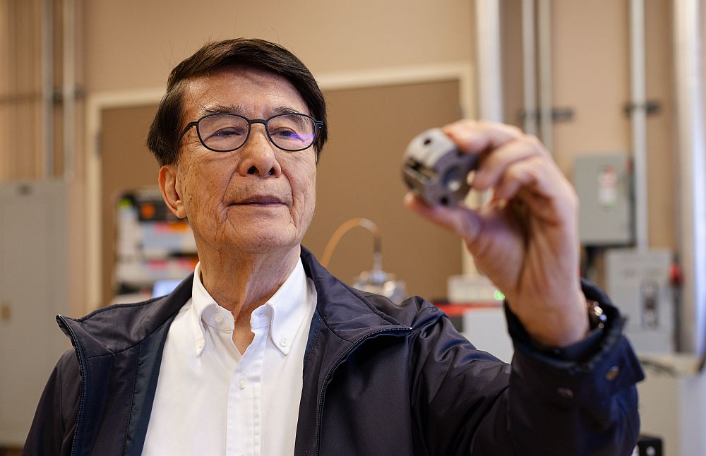
NIST announces new materials research center
The National Institute of Standards and Technology recently selected a consortium led by Northwestern University to establish a new NIST-sponsored center of excellence for advanced materials research. The new Center for Hierarchical Materials Design will be funded in part by a $25 million award from NIST over five years. The new center will focus on developing the next generation of computational tools, databases and experimental techniques to enable “materials by design,” one of the primary goals of the administration’s Materials Genome Initiative (MGI). Work will encompass both inorganic and organic advanced materials in fields as diverse as self-assembled biomaterials, smart materials for self-assembled circuit designs, organic photovoltaic materials, advanced ceramics and metal alloys. Other members of the consortium include the University of Chicago, the Northwestern-Argonne Institute of Science and Engineering (a partnership between Northwestern and the Department of Energy’s Argonne National Laboratory) and the Computation Institute (a partnership between the University of Chicago and Argonne.) The consortium also plans to work closely with QuesTek Innovations, a small business spin-off of NU; ASM International; and Fayetteville State University.
Researchers report shape memory in ceramics
Following on the announcement earlier this year of shape memory in zirconia, a research team at Lawrence Berkeley National Laboratory has discovered a way to introduce a recoverable strain into bismuth ferrite of up to 14% on the nanoscale. The effect, larger than any shape-memory effect observed in a metal, is said to open the door to applications in a wide range of fields, including medical, energy and electronics. Bismuth ferrite is a multiferroic compound that displays both ferroelectric and ferromagnetic properties, meaning it will respond to the application of external electric or magnetic fields. In this latest study, in addition to the conventional thermal activation, an elastic-like phase transition was introduced into bismuth ferrite using only an electric field.
Improved catalyst for solar-powered hydrogen production
Hydrogen burns cleanly and can generate electricity via fuel cells. One way to sustainably produce hydrogen is by splitting water molecules using the renewable power of sunlight, but scientists are still learning how to control and optimize this reaction with catalysts. At the National Synchrotron Light Source, researchers from Columbia University, Harvard University, and Brookhaven National Laboratory used X-rays to better understand the intermediate-range nanoscale structure of cobalt phosphate and cobalt borate thin films, two promising catalyst candidate materials. The scientists report that the borate films consist of 3–4 nm cobalt–oxygen clusters that stack neatly up to three layers deep. The phosphate films consist of significantly smaller clusters that do not stack in an ordered way. These structural differences seem to tie into the films’ catalytic activity: as film thickness increased, the borate films were more active than phosphate and ultimately displayed a “significantly superior” performance. The findings suggest that the increase in borate film thickness also increases the effective surface area available for catalysis, while at the same time preserving the charge-transport properties of the films, the scientists say.
Scientists develop ‘recipe’ for self-assembling single crystals
A Northwestern University research team has produced near-perfect single crystals out of nanoparticles and DNA. Although they worked with gold nanoparticles, the researchers say the general “recipe” for single crystal production allows unprecedented control over the type and shape of crystals that can be produced and can be applied to a variety of materials with potential applications in photonics, electronics, and catalysis, the scientists say. To achieve a self-assembling single crystal in the lab, the research team used two sets of gold nanoparticles outfitted with complementary DNA linker strands. Working with approximately 1 million nanoparticles in water, they heated the solution to just above the DNA linkers’ melting point and then cooled it to room temperature over a period of days. The very slow cooling process encouraged the single-stranded DNA to find its complement, resulting in a high-quality single crystal approximately 3 μm wide.
Semiconductor nanowires produce laser light at useful wavelengths
Semiconductor nanowires have potential as laser materials for applications in computing, communications, and sensing, according to scientists at the Technische Universität München. The III-IV semiconductor nanowires can be grown directly on silicon, presenting opportunities for integrated photonics and optoelectronics, and operate at room temperature. They are said to have a tailored core-shell structure that enables them to act both as lasers, generating coherent pulses of light, and as waveguides similar to optical fibers. Potential applications for nanowire lasers include on-chip optical interconnects or even optical transistors to speed up computers, integrated optoelectronics for fiber-optic communications, and laser arrays with steerable beams. Ongoing research is directed toward better understanding the physical phenomena at work in such devices as well as toward creating electrically injected nanowire lasers, optimizing their performance, and integrating them with platforms for silicon photonics.