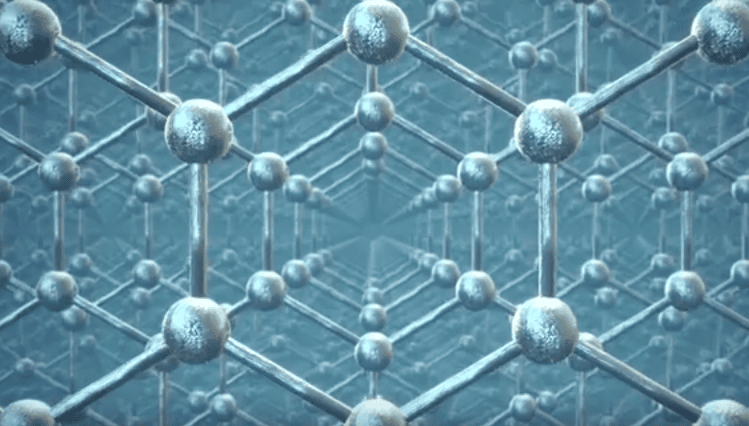
[Image above] Illustrative representation of the molecular structure of graphene. Credit: FW: Thinking’s video “Super-thing graphene means super power“; YouTube
What can’t graphene do?
It certainly seems the potential applications for this versatile material are endless. Graphene’s single-layer thickness, toughness, and supreme mechanical and thermal properties make it an ideal choice for developing electronic, optoelectronic, and electromechanical devices and sensors.
But scaling up commercially viable graphene for electronic and other applications has been complicated and expensive.
From creating defective graphene—which allows defects to be created within the material, altering its electrical and mechanical properties to make it more useful—to growing graphene nanoribbons—which helps harness graphene’s electronic properties in semiconductor applications—scientists are thinking outside the box when it comes to developing cost-effective ways to mass produce this wonder material.
So what’s been going on in the lab with graphene these days? Check out the latest graphene research news in brief.
Graphene teams up with glass to boost electronic properties.
This news hits closest to home for our ceramic and glass materials community. Scientists at the U.S. Department of Energy’s Brookhaven National Laboratory, Stony Brook University, and the Colleges of Nanoscale Science and Engineering at SUNY Polytechnic Institute developed a simple and powerful method for creating resilient, customized, and high-performing graphene: layering it on top of soda-lime glass.
“We believe that this work could significantly advance the development of truly scalable graphene technologies,” Matthew Eisaman, study coauthor and physicist at Brookhaven Lab and professor at SBU, says in a Brookhaven news release.
The sodium inside the soda-lime glass creates high electron density in the graphene, which is essential to many processes and has been challenging to achieve, coauthor Nanditha Dissanayake of Voxtel Inc. (formerly of Brookhaven Lab) explains in the release.

Left: Schematic of a graphene field-effect-transistor. The research revealed the soda-lime glass (SLG) substrate serves as a source of sodium doping and improved device performance in a way not seen in the sodium-free substrate. Right: A scanning electron micrograph of the device as seen from above, with the white scale bar measuring 10 microns and a transmission electron micrograph inset of the copper indium gallium diselenide (CIGS)/graphene interface where the white scale bar measures 100 nm. Credit: Brookhaven National Laboratory
The study, published in Scientific Reports, is “Spontaneous and strong multi-layer graphene n-doping on soda-lime glass and its application in graphene-semiconductor junctions” (DOI: 10.1038/srep21070).
But the headlines don’t stop at the partnership between graphene and glass.
Graphene is a metal that behaves like water.
Researchers at Harvard University recently found that “when the strongly interacting particles in graphene were driven by an electric field, they behaved not like individual particles but like a fluid that could be described by hydrodynamics,” according to a Harvard news release.
“Instead of watching how a single particle was affected by an electric or thermal force, we could see the conserved energy as it flowed across many particles, like a wave through water,” says first author Jesse Crossno, a graduate student in the Kim Lab at Harvard.
The paper, published in Science, is “Observation of the Dirac fluid and the breakdown of the Wiedemann-Franz law in graphene” (DOI: 10.1126/science.aad0343).
Graphene safely interacts with neurons in the brain for the first time, broadening the material’s potential biomedical applications.
Researchers at the University of Trieste in Italy and the Cambridge Graphene Centre at the University of Cambridge in the U.K. found for the first time that graphene can be used to make electrodes for implantation in the human brain, “which could potentially be used to restore sensory functions for amputee or paralyzed patients, or for individuals with motor disorders such as Parkinson’s disease,” according to a Cambridge news release.
“For the first time we interfaced graphene to neurons directly,” Laura Ballerini of the University of Trieste says in the release. “We then tested the ability of neurons to generate electrical signals known to represent brain activities, and found that the neurons retained their neuronal signaling properties unaltered. This is the first functional study of neuronal synaptic activity using uncoated graphene based materials.”
The study, published in ACS Nano, is “Graphene-based interfaces do not alter target nerve cells” (DOI: 10.1021/acsnano.5b05647).
Bonus: Ever wondered how to make graphene?
This video from Harvard’s John A. Paulson School of Engineering and Applied Sciences shows you how!