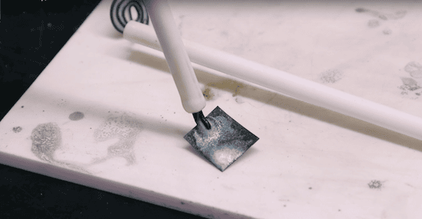
Archive for nanotubes

You are browsing the archives of nanotubes.

Other materials stories that may be of interest

MIT researchers improve efficiency of quantum-dot photovoltaic system by adding a forest of nanowires

Photovoltaics based on tiny colloidal quantum dots have several potential advantages over other approaches to making solar cells. But there’s a tradeoff in designing such devices because of two contradictory needs for an effective PV: A solar cell’s absorbing layer needs to be thin to allow charges to pass readily from the sites where solar energy is absorbed to the wires that carry current away—but it also needs to be thick enough to absorb light efficiently. Improved performance in one of these areas tends to worsen the other, says Joel Jean, a doctoral student in MIT’s Department of Electrical Engineering and Computer Science. The addition of zinc oxide nanowires can play a useful role, says Jean, who is the lead author of a paper to be published in the journal Advanced Materials. These nanowires are conductive enough to extract charges easily, but long enough to provide the depth needed for light absorption, Jean says. Using a bottom-up growth process to grow these nanowires and infiltrating them with lead-sulfide quantum dots produces a 50 percent boost in the current generated by the solar cell, and a 35 percent increase in overall efficiency, Jean says. The process produces a vertical array of these nanowires, which are transparent to visible light, interspersed with quantum dots.

Nanotubes boost potential of salinity power as a renewable energy source

(Gizmag) In November 2009, Norwegian state owned electricity company Statkraft opened the world’s first osmotic power plant prototype, which generates electricity from the difference in the salt concentration between river water and sea water. While osmotic power is a clean, renewable energy source, its commercial use has been limited due to the low generating capacities offered by current technology - the Statkraft plant, for example, has a capacity of about 4 kW. Now esearchers have discovered a new way to harness osmotic power that they claim would enable a 1 square meter (10.7 sq. ft.) membrane to have the same 4 kW capacity as the entire Statkraft plant. The global osmotic, or salinity gradient, power capacity, which is concentrated at the mouths of rivers, is estimated by Statkraft to be in the region of 1,600 to 1,700 TWh annually. Electricity can be generated through the osmotic phenomena that results when a reservoir of fresh water is brought into contact with a reservoir of salt water through the use of a special kind of semipermeable membrane in one of two ways—either by harnessing the osmotic pressure differential between the two reservoirs to drive a turbine, or by using a membrane that only allows the passage of ions to produce an electric current.

Don’t call it vaporware: Scientists use cloud of atoms as optical memory device

(NIST Tech Beat) Talk about storing data in the cloud. Scientists at the Joint Quantum Institute (JQI) of the NIST and the University of Maryland have taken this to a whole new level by demonstrating that they can store visual images within quite an ethereal memory device—a thin vapor of rubidium atoms. The effort may prove helpful in creating memory for quantum computers. Their work builds on an approach developed at the Australian National University, where scientists showed that a rubidium vapor could be manipulated in interesting ways using magnetic fields and lasers. The vapor is contained in a small tube and magnetized, and a laser pulse made up of multiple light frequencies is fired through the tube. The energy level of each rubidium atom changes depending on which frequency strikes it, and these changes within the vapor become a sort of fingerprint of the pulse’s characteristics. If the field’s orientation is flipped, a second pulse fired through the vapor takes on the exact characteristics of the first pulse-in essence, a readout of the fingerprint.

Recyclable solar cells made from trees

Fabricating new plant-based solar cells on cellulose nanocrystal substrates means that they’re recyclable in water. Researchers report that the organic solar cells reach a power conversion efficiency of 2.7 percent, an unprecedented figure for cells on substrates derived from renewable raw materials. The cellulose nanocrystal (CNC) substrates on which the solar cells are fabricated are optically transparent, which lets light pass through them before being absorbed by a very thin layer of an organic semiconductor. During the recycling process, the solar cells are simply immersed in water at room temperature. Within minutes, the CNC substrate dissolves and the solar cell can be separated easily into its major components. To date, organic solar cells have been typically fabricated on glass or plastic. Neither is easily recyclable, and petroleum-based substrates are not very eco-friendly. For instance, if cells fabricated on glass were to break during manufacturing or installation, the useless materials would be difficult to dispose of. ”Our next steps will be to work toward improving the power conversion efficiency over 10 percent, levels similar to solar cells fabricated on glass or petroleum-based substrates,” says Bernard Kippelen, a professor at the Georgia Institute of Technology’s College of Engineering, who led the study. The group plans to achieve this by optimizing the optical properties of the solar cell’s electrode.

A step toward optical transistors?

As demand for computing and communication capacity surges, the global communication infrastructure struggles to keep pace, since the light signals transmitted through fiber-optic lines must still be processed electronically, creating a bottleneck in telecommunications networks. While the idea of developing an optical transistor to get around this problem is alluring to scientists and engineers, it has also remained an elusive vision, despite years of experiments with various approaches. Now, McGill University researchers have taken a significant, early step toward this goal by showing a new way to control light in the semiconductor nanocrystals known as “quantum dots.” In results published online recently, researchers show that all-optical modulation and basic Boolean logic functionality—key steps in the processing and generation of signals—can be achieved by using laser-pulse inputs to manipulate the quantum mechanical state of a semiconductor nanocrystal. Quantum dots already are used in applications ranging from photovoltaics, to light-emitting diodes and lasers, to biological imaging. Patanjali (Pat) Kambhampati’s McGill group’s, latest findings point toward an important new area of potential impact, based on the ability of these nanocrystals to modulate light in an optical gating scheme. “These results demonstrate the proof of the concept,” Kambhampati says. “Now we are working to extend these results to integrated devices, and to generate more complex gates in hopes of making a true optical transistor.”

Nanotechnology imaging breakthrough

A team of researchers has made a major breakthrough in measuring the structure of nanomaterials under extremely high pressures. For the first time, they developed a way to get around the severe distortions of high-energy X-ray beams that are used to image the structure of a gold nanocrystal. The technique, described in Nature Communications, could lead to advancements of new nanomaterials created under high pressures and a greater understanding of what is happening in planetary interiors. Lead author of the study, Wenge Yang of the Carnegie Institution’s High Pressure Synergetic Consortium explains, “The only way to see what happens to such samples when under pressure is to use high-energy X-rays produced by synchrotron sources. Synchrotrons can provide highly coherent X-rays for advanced 3D imaging with tens of nanometers of resolution. This is different from incoherent X-ray imaging used for medical examination that has micron spatial resolution. The high pressures fundamentally change many properties of the material.” The team found that by averaging the patterns of the bent waves-the diffraction patterns-of the same crystal using different sample alignments in the instrumentation, and by using an algorithm developed by researchers at the London Centre for Nanotechnology, they can compensate for the distortion and improve spatial resolution by two orders of magnitude.

International team finds help from boron nitride nanotubes in cancer treatment

International team finds help from boron nitride nanotubes in cancer treatment


The first macroscopic, commercially usable BNNTs, spun into a 3-centimeter-long, 1-milimeter-diameter piece of yarn. Credit: Michael Smith.

Once again, we are reminded that not all scientifically interesting nanotubes are of the carbon variety. Researchers from a number of US and international institutions have released a new study that suggests that placing boron nitride nanotubes on the surface of cancer cells may be able to significantly improve one of the treatment options for soft-tissue cancers, such as those in the pancreas, liver, lung, brain and prostate.

The treatment is called Irreversible Electroporation and it is a relatively new and minimally invasive treatment for difficult-to-treat cancers in soft tissues that uses short pulses of high amplitude static electric fields to attack the cell walls of tumors. ”Irreversible Electroporation is a way of putting holes in the wall of a tumor cell,” says Michael W. Smith in a story on the Jefferson Lab website. Smith, now the chief scientist at BNNT LLC, was formerly a staff scientist at NASA’s Langley Research Center. ”The cell will literally go, ‘Oh, something’s terribly wrong,’ and kill itself. That’s called apoptosis,” he explains.

According to the Jefferson Lab story, Smith read about research being conducted at the Institute of Life Sciences, Scuola Superiore Sant’Anna in Pisa with BNNTs in a journal, and “he offered the researchers a sample of the very high-quality Jefferson Lab/NASA Langley/National Institute of Aerospace BNNTs. These BNNTs are highly crystalline and have a small diameter. Structurally, they also contain few walls with minimal defects, and are very long and highly flexible.”

Using the new BNNTs with in vitro samples, the Italian researchers found the IRE treatment method combined with BNNTs killed twice as many cancer cells (88 percent) on the tumor surface than without (40 percent).

“They were able to get, in a petri dish, more than double the effectiveness. So, this technique works twice as well with our nanotubes on the cells than without them” says Smith. Smith’s company acquired on March 22 the intellectual property rights for making the material available for scientific and commercial research, development and products.

The collaborators are now attempting to scale up the BNNT production process and improve their purity. They caution that their IRE/BNNT work is still very preliminary and say their next step will be studies in mice.

The BNNTs given to the Italian group were made, according to the Jefferson Lab story, using a pressurized vapor/condenser, where a laser aimed at at a boron target first creates boron gas. Then the gas is exposed to a condensor metal wire, which causes liquid boron droplets to form. These droplets combine with the nitrogen to self-assemble into BNNTs.

The work is featured in a paper in Technology in Cancer Research and Treatment.

Spinning yarn out of nano powder-infused nanotubes for superconducting applications

Spinning yarn out of nano powder-infused nanotubes for superconducting applications

Credit: Science/AAAS/UTD NanoTech Institute

Recently I wrote about Israeli-based TorTech, which says it will soon be manufacturing carbon nanotube fiber yarns that it claims to be stronger than Kevlar, yet still flexible and lightweight. While Tor-Tech plans to implement the technology for military use, spinning nano yarns has potential for many applications.

MIT’s Technology Review reported on research out of the University of Texas at Dallas, demonstrating a way to spin yarn out of nanotubes infused with nano powders. According to the article, the researchers have used the method to make strips of yarn that have a wide array of properties, allowing them to function in diverse applications, such as a battery electrodes, superconducting materials and self-cleaning yarns.

These fibers could solve a big practical problem: Powders without form are difficult to use, yet they are a very important component to functional materials because they have very high surface area. Sintering and binding are complicated processes typically used to give form to powder materials.

Ray Baughman, director of the MacDiarmid NanoTech Institute at the University of Texas at Dallas, says nano yarns should make it easier to work with a wide range of powdered materials. “You can take almost any powder and make a sewable, knittable, knotable, braidable yarn,” he tells Technology Review.

According to the article:

The researchers start by growing a forest of vertically aligned carbon nanotubes in a chemical reactor. Then they drag a roller over the nanotubes, which separate from the surface and get tangled up in a long, stretchy ribbon — a so-called nanotube web . . . The researchers spray the surface of the web with the powder and then twist it into a yarn. The powder is confined inside the spirals of the nanotube web. “When you wash it, almost all the powder is retained,” he says. The resulting yarns can be 95 to 99 percent powder by weight.

Baughman’s group used a mixture of powdered boron and magnesium to make superconducting yarns by a simple process. The conventional process for making superconducting wires involves packing the powders in copper tubes and heating and drawing them tens of times to stretch them into wires. But the superconducting yarns are heated just once to anneal the powders and form a superconducting thread.

Some applications in which Baughman has applied the technology includes battery-electrode fabric using lithium-iron-phosphate powders. Since the fabric is about 99 percent active material, he thinks it could be used to make less-heavy batteries. The yarns could also be used to produce material for structural manufacturing.

On the NanoTech Institute’s website, researchers note, “We have spun carbon nanotube composite fibers at a hundred times the prior-art rate, and obtained fibers that pound-per-pound have twice the strength and stiffness and 70 times the toughness of strong steel wire. In addition to other functionalities, we have used these fibers for both electrical energy transmission and sensor devices in electronic textiles.”

First, its important to find appropriate markets. “Right now it’s more sensible to talk about batteries, not airplane wings, because of the tonnage [of materials] required,” says Baughman.

The powers can be applied via spraying techniques or even using inject printing A video demonstrating titanium dioxide powder being sprayed onto a moving nanotube web can be viewed on MIT’s website here.


Materials stories that may also be of interest

At the end of each week, I end up with a list of a bunch of stories I started to write about, or started to investigate or didn’t even get that far even though the topic looked intriguing, but, I had a meeting to go to …

Anyway, it’s Friday, and rather than have these stories evaporate into the ether, I’ve close out each week by providing some raw links to some of these orphan tales. Check ‘em out:

VCU Researchers May Have a New Class of Highly Electronegative Chemical Species

Yale scientists trick bacteria into incorporating foreign small molecules and embedding them within the cell wall.

Kinetics of fiber solidification, such as solidification kinetics of nanotube composite fibers (PNAS paper)

Fundamental limit of nanophotonic light trapping in solar cells (PNAS paper)

Particle size matters more than previously thought in crucial redox reactions

Ceramic science stories we missed the first time around

Weddings, vacation, illness, travel days . . .  Looking back, sometimes there have been events that caused us to miss a few good ceramic- and glass-related developments and press releases. The stories in this grab bag have only a few cobwebs on them, so check ‘em out:

Cementing success: Startup that eyes radical shift in cement industry wins MIT $100K business-plan competition

Closing in on a carbon-based solar cell

Better boron nitride nanotubes may be on the way

Lasers at the cutting edge of science

Japanese company develops world’s first ultra-thin piezoelectric waterproof speaker

Murata Supplying World’s Smallest 0402*-Size 10μF 6.3V-Rated Monolithic Ceramic Capacitor

Nanospheres stretch limits of hard disk storage

and, a video from Onyx Solar: Paving the way for building integrated photovoltaics: