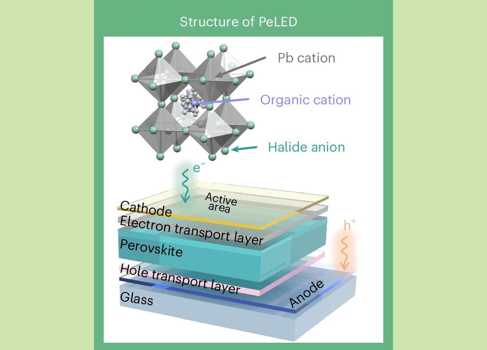
[Image above] Illustration showing the structure of a perovskite light-emitting diode. Credit: Zhang et al., Nature Sustainability (CC BY 4.0)
Perovskite solar cells have received a lot of attention in the past few years, including within CTT (see our latest coverage at the links here, here, and here). Recent developments have advanced this technology to the point that it is now being commercialized.
But perovskites are also showing promise for another application: light-emitting diodes (LEDs). When this family of materials is used as the light-emitting layer in LEDs, potential advantages include a wider color range, exceptional brightness, lightweight design, flexibility, abundant raw materials, and low-cost fabrication, in contrast to some of the primary materials currently used.
The first perovskite LED was developed in 2014 by University of Cambridge researchers and colleagues using metal halide perovskites. Since then, the external quantum efficiency (EQE) of perovskite LEDs, or the percentage of electrical energy successfully converted into usable light, has continued to improve, particularly across the three primary colors red, green, and blue.
These improvements were made possible through the introduction of other newer technologies, such as quantum dots and nanocrystals, as well as strategies that support operational stability. Other methods for improving perovskite LED efficiency are discussed at the links here and here.
In addition to solid-state lighting and displays, potential applications of perovskite LEDs include visible light communication, wearable electronics, and lasers. However, there are still some hurdles to overcome before perovskite LEDs are commercialized. The following sections shine light on what is needed to realize this technology’s commercial potential.
The thicker the better: Developments toward higher efficiency and improved stability
Conventional perovskite LEDs typically have perovskite emissive layers with thicknesses between 10 and 40 nm. While this recipe has yielded high EQEs in the laboratory, the thin stacks are susceptible to nanometer-scale challenges, such as interface-dominated nonradiative recombination. They also leave little room to integrate internal optical elements without disrupting the charge balance.
Thicker emissive layers (above 50 nm) can result in higher light outcoupling efficiency, i.e., the fraction of internally generated photons that successfully escape out of the device (this type of efficiency contributes to the total EQE). They also allow integration of internal optical elements or multilayer barriers without disrupting charge balance.
A recent comprehensive review paper by scientists in China and the Republic of Korea looked at advances in thick perovskite LEDs. They organized these advances around the physics, materials, and architectures of perovskite LEDs.
Physics
Photon recycling, or where emitted photons are reabsorbed and re-emitted, can effectively lengthen the optical path (the distance light travels through an optical system). A longer path means more interaction time with the photons, which allows EQEs to be achieved far beyond the ray optics limit without additional optical outcoupling structures. With a major increase in thickness, the contribution of photon recycling to EQE also significantly increases.
A thicker LED also “lowers the average electric field and homogenizes its spatial distribution, which mitigates hot-spotting and field-assisted degradation,” writes the authors. However, ion mitigation strategies, such as ionic barriers or buffers at both contacts, are still required to avoid degradation.
Materials
Thermal evaporation and solution processing are two promising methods for fabricating thick perovskite emissive layers.
Thermal evaporation is a physical vapor deposition process that heats raw perovskite materials in a vacuum, causing them to vaporize and condense into a uniform coating over large areas. This vapor-phase strategy can reduce grain size, enhance crystallinity, and reduce defects, resulting in improved properties. Furthermore, compositional engineering during evaporation is effective in tailoring optoelectronic behavior (learn more in the following section on intergranular phase engineering.)
Solution-based deposition involves dissolving precursor materials or pre-synthesized nanocrystals in liquid solvents to create an “ink” that is then coated onto a substrate. This method is cost-effective, relatively simple, and also scalable. Various parameters can be tailored to achieve different compositions, crystal size, and interfacial chemistry while maintaining thickness. Passivation and photon-management elements can also be integrated directly during film formation.
The choice between these two methods is a trade-off between film quality and manufacturing economics, conclude the authors.
Architecture
Device designs involve other factors besides physical thickness, including how charge carriers are injected, transported, and recombined within the material’s energy paths. Recombination occurs within the bulk region instead of the interfaces, which allows suppression of nonradiative losses and mitigation of efficiency roll-off (i.e., when EQE decreases as the brightness or current density increases).
To maintain both charge balance and a uniform internal field, strategies include higher-mobility transport layers and thickness partitioning (i.e., compositional grading via interlayers and self-assembled monolayers). Surface texturing using dome-shaped nanostructures can increase the outcoupling efficiency significantly.
The authors conclude that moving to thick perovskite architectures “necessitates a design paradigm shift from focusing solely on geometric thickness to actively engineering the optical thickness.”
With continued advancements, thick-film perovskite LEDs “are well placed to enter the mainstream of flexible electronics…for next-generation displays, solid-state lighting, and wearable systems,” the authors write.
The paper, published in Small, is “Beyond thin stacks: Physics, materials, and architectures of thick perovskite light-emitting diodes” (DOI: 10.1002/smll.202512877).
Intergranular phase engineering helps achieve record efficiency
Large-area perovskite LEDs are limited by severe performance losses as a result of grain boundary defects and nonuniform film formation. These problems must be overcome before such LEDs are suitable for commercial display and lighting technologies.
One solution to defect passivation is the incorporation of zinc-containing additives. These additives can form interphases that bridge adjacent perovskite grains, thereby suppressing trap-assisted recombination, directing preferential crystal orientation, and enhancing environmental stability.
In a recent paper, researchers at Jilin University in China added ZnBr2 during film formation to produce Cs2ZnBr4 interphases in CsPbBr3 films. Analysis showed that these interphases resulted in smoother, more homogeneous perovskite films with reduced morphological disorder.
Thanks to the enhanced crystal orientation, the researchers successfully fabricated large area quasi-2D perovskite LEDs with an active area of 2.25 cm2. These LEDs exhibited EQEs of 25.2% for green emission at 516 nm and 23.7% for red emission at 640 nm, which are the highest values reported to date for devices of this scale, according to the authors. Additionally, the emission wavelength for the green LEDs remained consistent across the entire film.
Besides improvements in EQE, the addition of ZnBr2 also enhanced device reproducibility and environmental stability. The authors concluded that “intergranular phase engineering [is] a scalable and robust strategy toward practical, high-performance perovskite light-emitting technologies.”
The paper, published in ACS Energy Letters, is “Bridging grains with Cs2ZnBr4 enables record 25.2% EQE large-area perovskite LEDs” (DOI: 10.1021/acsenergylett.6c00048).
Assessing environmental and economic performance from cradle to grave
As with any new technology heading toward commercialization in today’s world, modern manufacturers are keenly aware of the need to produce perovskite LEDs in an environmentally friendly manner. Accomplishing this goal means taking a closer look at the technology’s raw material acquisition, manufacturing, distribution, use, and end-of-life pathways.
Researchers led by Linköping University in Sweden recently investigated the life-cycle impacts of 18 representative perovskite LEDs (only the light-emitting components) spanning red, green, blue, white, and near-infrared wavelengths. Most of these devices were made from similar raw materials, and most had comparable environmental impact profiles.
In general, the environmental impacts of the representative LEDs stemmed primarily from the inputs of substances and electricity during production. In particular, electricity consumption accounted for more than 99% of the impacts during device assembly. In contrast, transport accounted for less than 5% of total impacts.
Regarding near-infrared devices, having gold cathodes in the LED increased the environmental impacts by more than 100 times due to the high energy consumption and pollution associated with mining gold. The authors estimate that replacing gold with aluminum, copper, or nickel could reduce the impacts of near infrared LEDs by three orders of magnitude.
For all perovskite LEDs, heavy metals were major contributors throughout the life cycle. However, lead’s contribution to total toxicity is minimal compared to other pollutants because only a thin layer is used in the device (typically only tens of nanometers).
The researchers gave multiple examples of how recycling could benefit future industrial applications by reducing raw material input. For instance, they noted that reusing organic cleaning solvents reduced environmental impact by nearly 60%. By also recycling metal electrodes and glass substrates, commercial LEDs could reduce their environmental impact by up to 90% compared to laboratory devices, according to the researchers.
The researchers developed a new parameter called “relative impact mitigation time” to quantify the lifetime required to achieve sustainability. This parameter estimates the minimal time required to mitigate relative impacts by accounting for internal and external relative impacts simultaneously. Using this parameter, the researchers determined that a lifetime on the order of 10,000 hours was needed to offset environmental impacts.
Cost of future technology was expected to be comparable to that of current commercial organic LED panels (around $100 per square meter). The researchers believe that once large-scale manufacturing is achieved, perovskite LEDs will be “competitive among various lighting technologies from both environmental and economic perspectives.”
The open-access paper, published in Nature Sustainability, is “Towards sustainable perovskite light-emitting diodes” (DOI: 10.1038/s41893-024-01503-7).