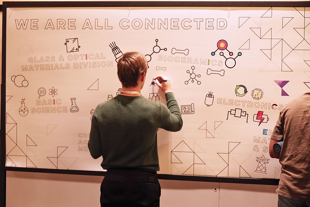
Other materials stories that may be of interest
Interdisciplinary team demonstrates superconducting qualities of topological insulators
Topological insulators (TIs) are an exciting new type of material that on their surface carry electric current, but within their bulk, act as insulators. Since the discovery of TIs about a decade ago, their unique characteristics (which point to potential applications in quantum computing) have been explored theoretically, and in the last five years, experimentally. But where in theory, the bulk of TIs carry no current, in the laboratory, impurities and disorder in real materials mean that the bulk is, in fact, conductive. This has proven an obstacle to experimentation with TIs: findings from prior experiments designed to test the surface conductivity of TIs unavoidably included contributions from the surplus of electrons in the bulk. Now an interdisciplinary research team at the University of Illinois at Urbana-Champaign, in collaboration with researchers at Brookhaven National Laboratory’s Condensed Matter Physics and Materials Science Department, has measured superconductive surface states in TIs where the bulk charge carriers were successfully depleted. To deplete the electrons in the bulk, the team used three strategies: the TI material was doped with antimony, then it was doped at the surface with a chemical with strong electron affinity, and finally an electrostatic gate was used to apply voltage that lowered the energy of the entire system.
UD researchers receive additive manufacturing funds
The University of Dayton Research Institute will benefit from the first round of applied research and development project awards the National Additive Manufacturing Innovation Institute announced in a few weeks ago. Rapid Prototype + Manufacturing LLC of Avon Lake, Ohio, was awarded $1 million for “Maturation of Fused Deposition Modeling Component Manufacturing,” and will contract with UD’s Research Institute for $575,000 for technology support and education. Other partners in the program, designed to resolve issues that have inhibited the transition to manufacturing of Fused Deposition Modeling, a popular thermoplastic-based additive process, include Stratasys of Eden Prairie, Minn., as well as aerospace companies Boeing, GE Aviation, Lockheed Martin and Northrop Grumman. “This program allows us to pool resources and leverage highly developed composites industry design practices to mature FDM manufacturing for aerospace and defense applications,” says Brian Rice, head of the Research Institute’s Multi-Scale Composites and Polymers Division. “UDRI’s role will be to analyze material properties and define how to design and certify parts manufactured for aerospace applications.” In July 2012, UDRI received $3 million from the Ohio Third Frontier to work with Stratasys, RP+M and additional partners to develop aircraft-engine components through additive manufacturing —also known as 3D printing—for several aerospace manufacturers.
New research shows ‘perfect twin boundaries’ are not so perfect
Eliminating the defects at the interface separating two crystals, or grains, has been shown by nanotechnology experts to be a powerful strategy for making materials stronger, more easily molded, and less electrically resistant-or a host of other qualities sought by designers and manufacturers. Since 2004, when a seminal paper came out in Science, materials scientists have been excited about one special of arrangement of atoms in metals and other materials called a “coherent twin boundary” or CTB. Based on theory and experiment, these coherent twin boundaries are often described as “perfect,” appearing like a perfectly flat, one-atom-thick plane in computer models and electron microscope images. But new research now shows that coherent twin boundaries are not so perfect after all. A team of scientists at the University of Vermont’s College of Engineering and Mathematical Sciences and the Lawrence Livermore National Laboratory and elsewhere report that coherent twin boundaries found in copper “are inherently defective.” With a high-resolution electron microscope, using a more powerful technique than has ever been used to examine these boundaries, they found tiny kink-like steps and curvatures in what had previously been observed as perfect. Even more surprising, these kinks and other defects appear to be the cause of the coherent twin boundary’s strength and other desirable qualities. “Everything we have learned on these materials in the past 10 years will have to be revisited with this new information,” says UVM engineer Frederic Sansoz.
DOE has issued request for information regarding rotating disk electrode diagnostics for PEMFC electrocatalyst screening
The DOE’s Fuel Cell Technologies Office has issued a request for information seeking feedback from interested stakeholders regarding the use of rotating disk electrode (RDE) experiments and best practices for experimental conditions for characterization of the activity and durability of proton exchange membrane fuel cell oxygen reduction reaction (ORR) electrocatalysts. A review of recent literature shows that the determination of the ORR activity has numerous intricacies that have not been systemically cataloged, resulting in values for the activity of Pt/C that vary significantly. Next steps will be to establish standard procedures and measurement parameters for the RDE technique so that novel catalysts can be benchmarked for ORR activity versus an accepted Pt/C baseline for polymer electrolyte fuel cell applications. DOE is specifically interested in information on best practices/protocols to enable consistency in procedures and less variability in results from different laboratories.
Researchers design nanometer-scale material that can speed up light to “infinitely fast” pace
In a process comparable to squeezing an elephant through a pinhole, researchers at Missouri University of Science and Technology have designed a way to engineer atoms capable of funneling light through ultra-small channels. Their research is the latest in a series of recent findings related to how light and matter interact at the atomic scale, and it is the first to demonstrate that the material—a specially designed “meta-atom” of gold and silicon oxide—can transmit light through a wide bandwidth and at a speed approaching infinity. The meta-atoms’ broadband capability could lead to advances in optical devices, which currently rely on a single frequency to transmit light, the researchers say. ”These meta-atoms can be integrated as building blocks for unconventional optical components with exotic electromagnetic properties over a wide frequency range,” write Jie Gao and Xiaodong Yang, assistant professors of mechanical engineering at Missouri S&T, and Lei Sun, a visiting scholar at the university. The researchers created mathematical models of the meta-atom, a material 100 nanometers wide and 25 nanometers tall that combined gold and silicon oxide in stairstep fashion. In their simulations, the researchers stacked 10 of the meta-atoms, then shot light through them at various frequencies. They found that when light encountered the material in a range between 540 terahertz and 590 terahertz, it “stretched” into a nearly straight line and achieved an “effective permittivity” known as epsilon-near-zero. Effective permittivity refers to the ratio of light’s speed through air to its speed as it passes through a material. As light passes through the engineered meta-atoms described by Gao and Yang, however, its effective permittivity reaches a near-zero ratio. In other words, through the medium of these specially designed materials, light actually travels faster than the speed of light. It travels “infinitely fast” through this medium, Yang says.
Energy Department awards $16M for small businesses focused on energy technologies
Acting Secretary of Energy Daniel Poneman announced that DOE is awarding 88 grants to small businesses in 28 states to develop clean energy technologies with a strong potential for commercialization and job creation. These awards, totaling over $16 million in investments, will help small businesses with promising ideas that could improve manufacturing processes, boost the efficiency of buildings, reduce reliance on foreign oil, and generate electricity from renewable sources. Companies competing for these grants were encouraged to propose outside-the-box innovations to meet ambitious cost and performance targets. The small businesses receiving the awards are located in 28 states: Alabama, Arizona, Arkansas, California, Colorado, Delaware, Florida, Georgia, Illinois, Kentucky, Louisiana, Maryland, Massachusetts, Michigan, Missouri, Montana, Nevada, New Hampshire, New Jersey, New Mexico, New York, Ohio, Pennsylvania, Tennessee, Texas, Utah, Virginia, and Washington. Companies competing for these grants were encouraged to propose outside-the-box innovations to meet ambitious cost and performance targets. The selections are for Phase I and Fast Track (combined Phase I and II) work. That means that the new projects will go toward exploring the feasibility of innovative concepts that could be developed into prototype technologies. Seventy-nine awards will go to SBIR projects, and another nine will go to STTR projects.
Strong, tough, and uncrushable—How Mother Nature designs structural biological materials
Nature is replete with ingenious structures to make life not just possible, but better. The bony plates of seahorse skeletons, for example, slide past each other, giving the creature incredible flexibility. Materials scientists at the University of California, San Diego, are working to unlock the secrets. Credit: Joanna McKittrick, UCSD.
The Materials Genome Initiative boosted the idea of “materials by design” to the forefront, giving it a name and a cause—reduce the timeline from material discovery to manufacture by half. Without getting into theological or philosophical arguments, Nature may be way ahead of us on executing the idea of materials by design, and the “cause” is simple: survival.
Nature has designed some ingenious materials. Spider thread, for example, has amazing tensile and stretching properties. Abalone shells resist the erosion of ocean floor environments that polish materials with similar compositions into shiny, pretty baubles prized by artists. Why don’t bird beaks break? How is the structure of seahorse spines an advantage?
University of California, San Diego, researchers Marc Meyers and Joanna McKittrick, and Po-Yu Chen, now at National Tsing Hua University, Taiwan—recently wrote a review article in Science (subscription required) on the mechanics of structural biological materials. Specifically, they were looking for the connection between the structure and properties of biological materials, with an eye toward understanding how to engineer similar structures and properties in synthetic materials. Their review focused on three properties: strength under tension, toughness, and resistance to buckling/torsion.
First, they note that there are seven distinguishing characteristics of structural biological materials: self assembly, multifunctionality, hierarchy (different structures at different scales for different purposes), hydration, mild synthesis conditions (low temperature and pressure in aqueous environments), constraints imposed by evolution and environment, and self-healing ability.
Biological materials fall into two broad structural categories: “soft” structures, which are non-mineralized, and “hard” structures, which are composites of minerals and fibrous organic biopolymers. Examples of the former include collagen, keratin, elastin, chitin, lignin, and others. Mineralized composites, the latter group, consist of a mineral reinforcement phase such as hydroxyapatite, calcium carbonate, or siica, embedded in a biopolymer matrix, such as collagen or chitin.
Examples from nature provide insights into the mechanics of structural biological materials. In a press release, McKittrick says, “Mother Nature give us templates. We are trying to understand them better so we can implement them in new materials.”
Besides properties, biological materials have secrets to reveal regarding processing. Exoskeletal animals, like abalones, grow their shells one layer at a time. McKittrick observes in the press release that 3D printing is basically the same concept. “You could build a material similar to the abalone shell using principles we learned from nature by printing layer upon layer of mineral deposits—and do it much faster than nature would.”
Like engineered materials, biological materials bring different properties to the task. “The mechanical behavior of biological constituents and composites is quite diverse,” the authors write. The stress-strain behavior of biominerals, for example, is linear. However, biopolymers behave in a nonlinear fashion, and are key contributors to the high tensile strength of biological materials. Deformation happens first with a stiffening process involving molecular uncoiling and unkinking. After the fibers are fully extended, the polymer backbone stretches and accommodates quite a lot of strain before rupture. Spider silk is a good example of a biopolymer that deforms, yet is strong.
If you are alive, you’ve got to be tough, too. According to the paper, “Toughness is defined as the amount of energy a material absorbs before it fails.” That is, tough materials can deform quite a lot and are strong. They employ several toughening mechanisms that take advantage of the nature of interfaces, for example, by interrupting crack propagation, deflecting cracks, or bridging gaps created by cracks. Examples of tough biological structures include lobster shells, antler bones, abalone nacre, and silica sponge.
Finally, Nature has tricks to share regarding structures that resist bending, torsion, and buckling and the necessary tradeoff between bending and buckling resistance. She does this with thin solid shells filled with lightweight foam or internal struts. This way structural integrity is maximized and the “weight penalty” is minimized. Examples from the plant world include bamboo and the giant bird of paradise stem. The animal world offers structures such as porcupine quills, feathers, and beaks. Skeletal bones, too, are structured with a solid external “cortical bone” sheath filled with a cellular “cancellous bone” core.
Besides structural biological materials, there are other familiar applications of bioinspired materials. For example, most are familiar with the invention of Velcro being inspired by the way plant burrs stuck to animal fur. Olympic sports fans may recall hearing about high-performance swimsuits (eventually banned from competition) that mimic the structure of shark skin and reduce drag in the water. New super-adhesive surgical tapes are designed after gecko foot structure.
“There are a tremendous number of examples of things we can’t do with traditional materials,” McKittrick says in the press release. She admits it will take time, “But they will be better.”
Who better than Mother Nature would know about genomes and design of materials!
If you are attending the PACRIM-GOMD conference in a few weeks, stop by ‘Symposium 23: Advances in Biomineralized Ceramics, Bioceramics, and Bioinstpired Designs,’ which McKittrick and Chen helped organize.
The paper is “Structural Biological Materials: Critical Mechanics-Materials Connections,” by Marc André Meyers, Joanna McKittrick, and Po-Yu Chen. Science, 15 February 2013 (DOI: 10.1126/science.1220854).
U Dayton establishes new CETRASE thin-films center
Officials at the University of Dayton announced that the school has created a new research center focused on various thin-film investigations and applications. The initiative, dubbed the Center of Excellence in Thin-Film Research and Surface Engineering (CETRASE), hopes to deliver significant breakthroughs in everything from fuel and solar cell to optics, sensors, and electronics.
In a UD press release, Guru Subramanyam says, ”We want to find ways to make better, more efficient, cost-effective sensors, electronics, electro-optics, and energy systems and hopefully create new jobs in the region.”
Subramanyam, who is currently serving as leader of CETRASE, is chair of UD’s electrical and computer engineering department, and is one of several CETRASE faculty “team” members. The school says team members come also come for UD’s departments of materials engineering, biology, and physics as well as the electro-optics graduate program and the University of Dayton Research Institute.
Subramanyam says CETRASE provides the opportunity to move from ad hoc collaborations to strategic efforts and the pursuit of funding. “It makes sense for us to put our heads together for a center where we can coordinate activities, interact and share common equipment and costs. We also will have strength in numbers when submitting proposals as part of a center,” he says in the release.
In an interview, Subramanyam says before CETRASE was formed, “We had our own separate projects, funding applications and supporters. One or two of us would collaborate if we discovered an overlap, but as a group we didn’t come together until now. Now, for the first time, we will be developing joint priorities and funding proposals. Focusing on joint activities will be a change for us, but as a united group, I think we will be more attractive to funding agencies.”
“In addition,” Subramanyam continues, ”we will be holding regular CETRASE events, such as monthly seminars and bringing in invited guest speakers.”
Subramanyam notes that CETRASE has already hired its first dedicated staff member, a PhD who will serve as a coordinator of the center’s activities.
When I asked Subramanyam if CETRASE has any projects that might be of particular interest to the ceramics community, he says, “We have quite a bit of ceramic-related work going on, such as barium strontium titanate thin films for tunable dielectrics, yttrium barium copper oxide thin films and vanadium oxide research for the Air Force.”
He says that one immediate benefit is that CETRASE participants have access to team members’ advanced laser sources, pulse laser deposition systems, SEMs, TEMs, X-ray diffraction and Raman spectroscopy equipment, magnetron sputtering systems, and photolithography tools.
University spokesperson Shawn Robinson tells me UD’s materials engineering research currently ranks second in the nation based on research dollars.
Covaron gains $300,000 in seed-stage funding for thermosetting ceramics tech
A unique Michigan-based startup company that is attempting to leverage a proprietary method of what it describes as thermosetting ceramics is on something of a roll. Covaron Advanced Materials (formerly called Kymeira Advanced Materials, as in the above video) announced that it has just secured $300,000 in seed money from a variety of sources, this after winning a $25,000 prize last November in the Accelerate Michigan innovation contest.
The idea of a thermoset ceramics isn’t entirely new. For example, several patents discuss thermosets and ceramic composite materials, and the Navy has a 2004 patent for a method of making boron-carbon-silicon ceramic using thermosetting polymers.
The main person behind the invention of Covaron’s technology is Vincent Alessi, an Oberlin College graduate whom is describes as “a serial inventor in the areas of material chemistry, medical devices, fluid dynamics, and neuroscience.”
Alessi has been able to surround himself with several people of considerable experience in the materials business world, including former Walmart sustainability manager Cameron Smith (featured with Alessi in the video), as well as Dave Hatfield, who helped commercialize thermoplastics technology at Dow Chemical, and Reed Shick, previously the intellectual capital manager for Dow R&D.
I had a chance to speak with Hatfield, the Covaron CEO, who tells me they aren’t anxious to publish research on the papers until a number of intellectual property safeguards are in place. He said Alessi has several patents pending on the technology. He also says Covaron is attempting to develop the technology as a platform to develop a number of unique materials, the first of which has been given the Petraforge brand by the company.
Covaron’s website says Petraforge “has physical properties similar to advanced ceramics yet eliminates the need for heat sintering at 3,600°F.” It goes on to say that Petraforge is “specially formulated to provide the strength, heat conductivity, and abrasion resistance needed to create long lasting patterns and molds for plastics and cast metals.”
When I pressed him for some details about the composition of the Petraforge or other materials, Hatfield deferred to the company’s official description: “[It is a] polymetallic oxide with a nominally amorphous polymeric (glassy) microstructure. … Covaron formulates multiple types of two-component systems, comprising an “A” and a “B” side, similar to thermosetting polymers such as two-part epoxies. … The “A” side is primarily made up of inorganic compounds. Low cost fibers such as glass or carbon can be added to improve strength and alleviate brittleness. The “B” side includes liquid reactants. These components are combined and first undergo a gelation followed by a unique “chemical sintering” reaction, progressing from a liquid phase, to a “green” phase, and then to a low temperature cure process.”
Hatfield said the curing takes place between 160°C and 210°C and can require several hours. The company claims that in regard to certain properties, such as flexural strength, compressive strength-to-weight ratio and thermal stability, its materials are on par with silicon carbide and alumina.
One obvious benefit in regard to traditional advanced ceramic approaches would be considerable manufacturing savings from not having to sinter, but the company also says the pre-cured material is like cake batter and can be molded into any shape. Hatfield says post-cured material is easily machined and not nearly as brittle as some ceramics.
The company also claims, “more than 70 percent of the raw materials used in Covaron products can come from industrial waste sources.”
Hatfield tells me that Covaron will use the $300,000 seed funding to further the characterization of the materials, perfecting the mold and pattern making application techniques (for use in plastic injection molding, metal sand casting, etc.) and laying the groundwork for an “A” round of venture capital infusion of around $2.5-$5 million targeted for the end of 2013 or early 2014.
Current investors include Mercury Fund in Houston, Texas; First Step Fund in Detroit, Michigan; Huron River Ventures in Ann Arbor, Mich. and Two Seven Ventures in Denver, Colo. According to a story in Crain’s Detroit Business, Hatfield asked one of the leaders of Two Seven Ventures, Dave Cornelius, to do some initial investigation of Alessi’s technology based on Cornelius’ previous stint as director of new ventures for Dow Corning.
Hatfield also mentions the company, at some future point, hopes to develop products for the oil and gas industry, such as proppants for fracking, and pipes and fittings. Could Covaron be another MesoCoat in the making? Stay tuned.
Other materials stories that may be of interest
How graphene and friends could harness the Sun’s energy
University of Manchester and National University of Singapore researchers have shown how building multi-layered heterostructures in a three-dimensional stack can produce an exciting physical phenomenon exploring new electronic devices. The breakthrough, published in Science, could lead to electric energy that runs entire buildings generated by sunlight absorbed by its exposed walls; the energy can be used at will to change the transparency and reflectivity of fixtures and windows depending on environmental conditions, such as temperature and brightness. Collectively, such 2D crystals demonstrate a vast range of superlative properties: from conductive to insulating, from opaque to transparent. Every new layer in these stacks adds exciting new functions, so the heterostructures are ideal for creating novel, multifunctional devices. The Manchester and Singapore researchers expanded the functionality of these heterostructures to optoelectronics and photonics. By combining graphene with monolayers of transition metal dichalcogenides (TMDC), the researchers were able to created extremely sensitive and efficient photovoltaic devices. Such devices could potentially be used as ultrasensitive photodetectors or very efficient solar cells. In these devices, layers of TMDC were sandwiched between two layers of graphene, combining the exciting properties of both 2D crystals. TMDC layers act as very efficient light absorbers and graphene as a transparent conductive layer. This allows for further integration of such photovoltaic devices into more complex, more multifunctional heterostructures.
Counting cracks in glass gives speed of projectile
A shattered windshield has a story to tell. The key to hearing it is counting the cracks. The number of cracks that emerge in a plate of glass or Plexiglas relates to the speed of the object that broke it, researchers demonstrate in Physical Review Letters. This simple relationship could prove useful for forensic scientists, archaeologists and even astronomers. Over the past century, most research into cracks has focused on parameters that determine whether a material remains intact when struck. Nicolas Vandenberghe and his colleagues at Aix-Marseille University in France decided to try something different: They wanted to push glass and other materials past their breaking points and study the resulting fractures. They wondered if they could connect the patterns of cracks to the properties of the impact that created them, something no one had done before, Vandenberghe says. So he and his team set up a shooting gallery. Knowing that cracks emerge within a matter of microseconds of impact, Vandenberghe employed a high-speed camera to capture the instant of collision. The photographic evidence revealed a clear connection: After taking into account the type of material and its thickness, the number of cracks doubled for every fourfold increase in the ball’s speed. For example, a 70-kph pellet caused an average of four cracks in 1-millimeter-thick Plexiglas plates, while a 280-kph one made eight.
Small in size, big on power: New microbatteries a boost for electronics
Though they be but little, they are fierce. The most powerful batteries on the planet are only a few millimeters in size, yet they pack such a punch that a driver could use a cellphone powered by these batteries to jump-start a dead car battery—and then recharge the phone in the blink of an eye. Developed by researchers at the University of Illinois at Urbana-Champaign, the new microbatteries out-power even the best supercapacitors and could drive new applications in radio communications and compact electronics. “This is a whole new way to think about batteries,” says William P. King, a Bliss Professor of mechanical science and engineering. “A battery can deliver far more power than anybody ever thought. In recent decades, electronics have gotten small. The thinking parts of computers have gotten small. And the battery has lagged far behind. This is a microtechnology that could change all of that. Now the power source is as high-performance as the rest of it.” With currently available power sources, users have had to choose between power and energy. For applications that need a lot of power, like broadcasting a radio signal over a long distance, capacitors can release energy very quickly but can only store a small amount. For applications that need a lot of energy, like playing a radio for a long time, fuel cells and batteries can hold a lot of energy but release it or recharge slowly.
Successful launch of the new materials institute at Queen Mary
Professor Jeremy Kilburn (vice-principal for science and engineering) and Professor Martin Dove (director) launched the new Materials Research Institute at Queen Mary, University of London, on April 15, 2013. The afternoon consisted of talks from Queen Mary academics and internationally-acclaimed experts, who presented recent developments in the area of materials research. The talks were followed by a reception held in the Queens’ Building Senior Common Room, and provided an opportunity for informal discussion and networking. The launch was a success, which received excellent feedback from visitors and colleagues.
India’s Defense Materials and Stores Research and Development organizes open house for students
In Kanpur, India, Defense Materials and Stores Research and Development (DMSRDE), a unit of Defense Research and Development Organization (DRDO), has been working in frontier area of non-matellic materials. To celebrate DRDO Technology Day, DMSRDE organised an open house for the students to show their products and technologies abilities. Around 500 students, along with their teachers from different schools, came to DMSRDE on this occasion to see the exhibition. The students therein saw different defense-related product, such as bullet proof jackets, coils used in the bofors gun, camouflage and stealth materials etc. DMSRDE is working in very important area of material development for high temperature structural applications. It has developed capabilities to produce the polycorbosilane precursor materials which are used in production of silicon carbide based strategic products. This material in turn can also be converted to high heat resistance silicon carbide fibers for composite development which have enormous applications in defence, atomic energy, and aerospace industries. It can withstand temperature between 1,500–2,000°C. These materials were displayed in the exhibition.
EU launches Remanence rare earth recycling project
The possible future restrictions to the supply of critical materials have been the subject of debate for several years. In response to these an international consortium has been brought together to develop new solutions to the European requirement for rare earth metals. Remanence is an ambitious program designed to dramatically increase the amount of rare earth materials recovered and remanufactured from existing waste streams. The project brings together European industry and academia across the supply chain to develop the innovative technologies, business models and market information required to exploit this valuable resource reducing dependence on primary sources. The partners will develop new and innovative processes for the recovery and recycling of neodymium iron boron magnets (NdFeB) from a range of waste electronic and electrical equipment (WEEE). Advanced sensing and mechanical separation techniques will be developed in combination with innovative processes to recover the rare earth magnets in the WEEE. Remanence brings together Europe’s leading experts in sensing, disassembly, recycling technology and materials processing in a multi-disciplinary project able to deliver significant technical advances. C-Tech Innovation Ltd will lead a consortium including University of Birmingham, Stena Technoworld AB, ACREO Swedish ICT AB, Leitat Technological Centre, OptiSort AB, Chalmers Industriteknik, Magneti Ljubljana and Kolektor Magnet Technology GMBH.
A more efficient jet engine is made from lighter parts, some 3D printed
(MIT Technology Review) A new generation of engines being developed by the world’s largest jet engine maker, CFM (a partnership between GE and Snecma of France), will allow aircraft to use about 15 percent less fuel-enough to save about $1 million per year per airplane and significantly reduce carbon emissions. The first of these new engine, called LEAP, will feature a technology that has never been used in a large-scale production jet engines before: ceramic composite materials that weigh far less than the metal alloys they’ll replace and can endure far higher temperatures. The engine will also make use of parts produced through 3D printing, a new kind of manufacturing that can produce complex shapes that would be difficult or impossible to make with conventional manufacturing techniques. These technologies could eventually be used to make more parts of the engine, leading to further advances in efficiency, says Gareth Richards, LEAP program manager for GE Aviation.


