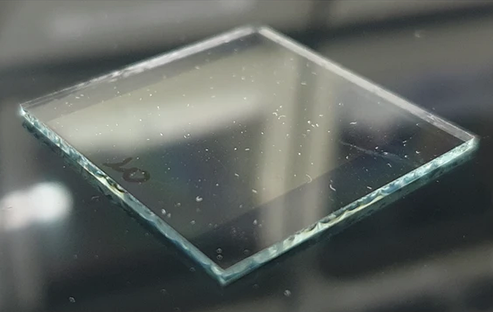
[Image above] A University of California, Berkeley group has a new method for growing semiconducting nanowire arrays on graphene that could lead to roll-out solar panels, flexible electronics, and more efficient batteries and supercapacitors for energy storage. Credit: Alper; University of California, Berkeley.
Can you imagine a “roll-out” solar cell? University of California, Berkeley graduate student John Alper can. His recent research on arrays of semiconducting nanowires grown on graphene substrates is a proof-of-concept step toward enabling roll-out solar cells and innovations for other technologies like rechargeable batteries and supercapacitors. Alper works in Roya Maboudian’s group in the department of chemical and biomolecular engineering at UCB.
Researchers have shown that the charge–discharge cycle in rechargeable batteries generates less mechanical stress using anodes made of silicon nanowire arrays than with graphite anodes. As a result, rechargeable batteries using Si-NW could have up to ten times the specific capacity of batteries with graphite anodes. Similarly, silicon carbide nanowire arrays may find use in field emission cathodes because of their high aspect ratio and low electron affinity.
These applications use nanowire arrays on rigid substrates, but what if the arrays could be mounted on a flexible substrate? For example, would it be an advantage for batteries or supercapacitors to be cylindrical rolls? (Yes, it turns out.) Roll-out solar panels could reduce labor and mounting hardware costs and drive the cost of solar energy downward. A November 2012 DOE SunShot report (pdf), “Photovoltaic (PV) Pricing Trends: Historical, Recent, and Near-Term Projections,” reports the installed cost of PV systems ranges from $4.86/W for large systems to $6.13/W for small systems, and that installation accounts for an increasing share of system costs.
Nanowire semiconducting arrays used in these types of advanced applications must have good electrical contact with their substrates, but they must also be transferable to the flexible substrate after being grown on and detached from a rigid substrate. Making a part in one location and installing it into a system at another location is common enough engineering practice, but doing it with nanoscale components presents challenges. Thus, there is the additional issue of scalability—processes need to be more than laboratory curiosities.
In an email, Alper says his interest in growing nanowires on graphene grew out of papers he was reading on next-generation materials for photovoltaics and batteries. Thinking about the materials science involved, he says, “issues with electrically contacting large arrays of nanowires with simple and scalable methods also played a role in inspiring this work.”
His work, reported recently in Nanoscale, demonstrates for the first time the ability to grow silicon or silicon carbide nanowire arrays directly on graphene using scalable processes. Also, he and his coauthors showed they could transfer the nanowire–graphene hybrid from one substrate to another while maintaining good electrical contact between the nanowires and the graphene.
Graphene substrates were grown by chemical vapor deposition, then “seeded” with metal catalysts to grow Si-NW or SiC-NW arrays—gold in the case of Si-NW and nickel for SiC-NW. The seeded substrates were placed in a furnace where the CVD process was adapted for nanowire growth.
Characterization of the arrays confirmed the nanostructured morphology, and cyclic voltammetry confirmed that arrays were electrically connected to the graphene. The team also succeeded in transferring the nanowire–graphene onto sapphire or PMMA film substrates. Alper says this work opens the possibility for developing “lightweight, flexible, and more efficient photovoltaics, thin film batteries, supercapacitors, and flexible electronics in general.”
I asked Alper what it felt like to be the first to report a breakthrough such as this. His response is a reminder that, while science researchers take pains to be objective, they are not disinterested. He says that before getting into the lab, he and coauthor Albert Gutes conducted a thorough literature search to ensure that this was new territory. Thus, he says, “Finding that it was still a breakthrough after completing the experimental portion and preparation of the manuscript was a great relief more than anything else.”
The paper is “Semiconductor nanowires directly grown on graphene—towards wafer scale transferable nanowire arrays with improved electrical contact,” by John P. Alper, Albert Gutes, Carlo Carraro, and Roya Maboudian; Nanoscale (DOI: 10.1039/c3nr00367a).
Author
Eileen De Guire
CTT Categories
- Energy


