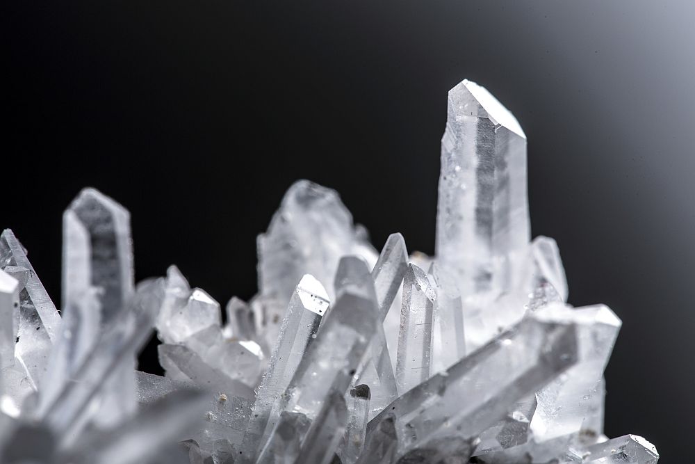
[Image above] Quartz, shown above, is a crystalline form of silica. It is abundant in the Earth’s crust, but finding deposits of high enough purity for electronic applications is challenging. Credit: Cagla Acikgoz / Shutterstock
Although rare earth metals and oil have dominated the headlines of global conflicts in recent months, there is another material lurking as the true gatekeeper of the modern age: ultrahigh-purity silica.
Since the Industrial Revolution, eras of human progress have been defined by how many decimal points of purity we can squeeze out of a grain of sand. Today’s CTT will focus on three relatively recent technological evolutions enabled by this globally scarce resource, starting with a personal story among the hedgerows of the Ardennes, where my granddad served as a combat engineer and tank commander with the Third Armored Division during World War II.
Evolution one: Optics (1810s–1950s)
At the time of my granddad’s service, Germany had the best optical technology in the world. While this gap in technology was partly due to Germany’s prowess in chemistry and physics, it also had to do with the country’s access to high-quality quartz sand supplies.
The Fontainebleau sand in France was the gold standard for European glass in the early years of the Industrial Revolution. This 99.7% pure silica sandstone allowed the German manufacturers, Zeiss and Leica, to dominate optical physics. The quality of German optics relied on this superior silica source and Ernst Abbe’s sine condition, which together with German chemical knowledge created their era of optical dominance.
Enter, stage left: geopolitics. During World War I, the Fontainebleau deposits remained under French control, thus cutting the Germans off for the duration of hostilities. I will not get into the many nuances of global politics, then or since, but suffice to say that the Germans learned their lesson and seized Fontainebleau soon after their invasion of France in 1940.
The fall of France left the Allies without a high-purity silica source. Furthermore, German optics manufacturers were producing gun sights and periscope lenses with a field of view larger than that of British, Russian, or U.S. lenses—providing a huge strategic advantage.
Fortunately, the Allies had a fallback position. The Lochaline sandstone deposit in Scotland had been known since the late 1800s, but due to its remoteness, it was not considered economically viable until 1940. However, the 99.8% pure silica under the Scottish basalt cliffs was leveraged during WWII to feed the Allied production of periscopes and tank sights. The underground deposits at Lochaline remained relevant for Cold War self-reliance, serving the mid-20th-century demand for glassware and laboratory equipment.
(Even as U.S. prominence in science and technology grew post-WWII, Germany still maintained high levels of innovation and research output. During the space race of the 1960s, my dad learned German so he could read source material for his double major in biology and chemistry—a decision that probably didn’t sit well with my granddad.)
Evolution two: Birth of the quartz crystal oscillator (1920s–1970s)
The next big technological leap for silica was its use in timekeeping. Walter Guyton Cady developed the first quartz crystal oscillator at Wesleyan University in the early 1920s, and the great size of WWII’s theaters of operation created a strong need for these oscillators to keep Allied radios on the same frequency and temporally coordinated.
At this time, the North Carolina mining district known as Spruce Pine first became strategic. Known today for its high-purity, electronic-grade quartz (learn more about that in the next section), Spruce Pine’s massive reserves of pegmatitic mica and quartz crystals were originally critical for military communications as insulators and oscillators, respectively.
Quartz crystal oscillators reached maturity in the 1970s with their use in electronic wristwatches. Although today some newer oscillator technologies have replace quartz in certain applications, quartz crystal oscillators retain their relevance as humans rekindle their interest in space exploration.
There is a whole school of thought around making communication in space possible. This topic becomes ever more relevant as the number of objects in low-Earth orbit increases. Satellite constellations need to be able to communicate effectively with one another, not just with the Earth, and quartz crystal oscillators remain the superior choice for phase noise performance and high frequency stability compared to some newer technologies.
Evolution three: The semiconductor revolution (1950s–today)
Knowledge of semiconducting effects started expanding in the mid-19th century, and by the 1930s, semiconducting materials were being used in early communications and radar equipment. Such devices were extensively used for range finding and targeting in WWII, but it was just after the war ended that semiconductor applications really took off with the invention of the first practical semiconductor device by Bell Lab scientists in 1947.
In 1958, Jack Kilby of Texas Instruments invented the first integrated circuit, paving the way for modern computing and electronics. Now, silicon semiconductors are integral to almost every electronic device, but the artificial intelligence boom is fueling demand for computer chips—and concurrently high-purity silica—like never before.
When I was researching the imperfect U.S. glass recycling system, I wondered whether recycled bottle glass could be used to meet the dramatically increasing need for silicon. Unfortunately, this idea is not possible due to the ultrahigh purity requirements for semiconductor silica. Fortunately for the U.S., the silica sources located at Spruce Pine are not just good for military communication applications—the site’s unique geology allows it to fulfill the demand for high-purity silica as well.
The 100-million-year advantage
Roughly 350 million years ago, the formation of the supercontinent Pangea pushed the area that is now Spruce Pine up to 15 miles underground. This forceful reorganization of the landscape created enormous heat and pressure, slowly melting the bedrock. Due the depths involved, water was almost completely absent in the melt. Therefore, associated impurities are also rare.
Even more slowly, the molten mass cooled. This 100-million-year annealing process formed massive, organized quartz crystals. The Spruce Pine deposit is technically a pegmatite, in contrast to the quartz sandstone deposits at Fontainebleau and Lochaline. Its unique conditions produced the highest purity natural quartz known on Earth, 99.999% silica (Five Nines or 5N). This quartz is critical to semiconductor production—specifically, the high-purity crucibles in which the silicon ingots are created.
Quartz crucibles: The sometimes overlooked key to Czochralski processing
The Czochralski method is the primary industrial process for growing the high-purity silicon ingots used to make semiconductor wafers. High-purity silicon is melted in a quartz crucible, and then a seed crystal is inserted and slowly pulled up while rotating, resulting in a solidified cylindrical ingot.
The silicon used for melting in the Czochralski method undergoes chemical refining beforehand to raise its purity. However, if a lower-purity quartz crucible is used for the Czochralski process—which takes place at temperatures above 1,400°C (nearly 2,600°F)—impurities within the crucible would leach into the melt. So, the crucible needs to be of a high purity as well to ensure no contamination during the Czochralski process.
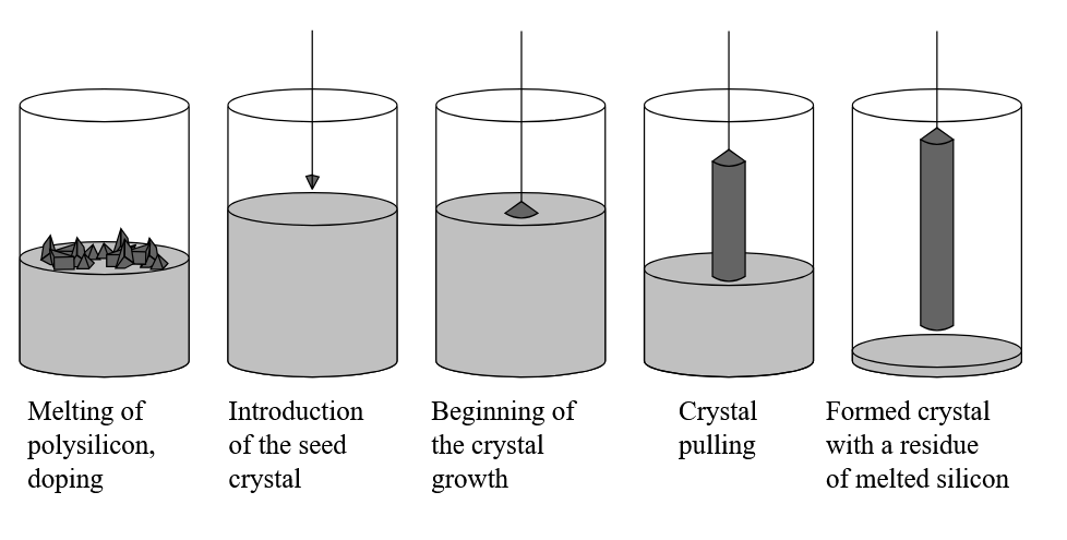
Illustration of the Czochralski process. Credit: Twisp, Wikimedia (public domain)
The largest portion of Spruce Pine’s output goes into the production of these single-use quartz crucibles. This mine alone accounts for roughly 70–90% of the global high-purity quartz supply for these crucibles.
The technical aspects of the Czochralski method notwithstanding, the process is as much art as it is science. Its practitioners, known as crystal growers, learn by apprenticing to master growers, and the technique takes a long time to perfect.
The story of computer chips is not quite complete once the silicon ingots are grown. Once the ingots are sliced into wafers, the semiconductor chips are patterned using photolithography, a method that uses light to transfer geometric patterns onto a substrate.
Netherlands-based ASML is the only manufacturer of extreme ultraviolet lithography machines, used for patterning chips at 5 nm and below. These machines use specialized mirrors and lenses that require synthetic fused silica—a direct evolution of the optical glass made by Zeiss (refer to the first section of this article). Because only ASML currently offers commercial patterning capabilities below 5 nm, it is the second critical bottleneck in advanced chip manufacturing.
Geopolitics (again)
Although Taiwan Semiconductor Manufacturing Company is the largest producer of chips, they are entirely dependent on Spruce Pine quartz for their crucibles. This U.S. monopoly of the crucible supply is the ace in the hole that balances the global semiconductor trade. If Spruce Pine stopped shipping today, the world’s advanced chip production would halt within months.
Despite billions in investment, China has not yet successfully produced advanced semiconductor-grade silicon at scale because they lack a Spruce Pine of their own. This fact provides a bargaining chip in the ongoing global maneuverings arising from China’s dominance in rare earth element production, as strategic mineral supplies are an important lever in global geopolitics.
My granddad’s tank sight optics and today’s advanced semiconductor chips are cousins. They are both chapters in the fascinating history of how humans learned to master the crystal lattice. We have come a long way, but in the end, we are all just the beneficiaries of a 100-million-year-old geological accident.