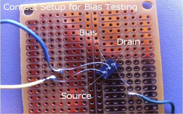
[Image above] Configuration for determining I-V curve of varistor–transistor hybrid devices as a function of applied bias voltage. Credit: Pandey, TSU
Chances are you know what a transistor is—“a semiconductor device used to amplify and switch electronic signals and electrical power,” according to Wikipedia’s crowdsourced experts.
But why it is called a “transistor” instead of something else? Apparently, six names were proposed for the revolutionary device discovered in 1947 by William Shockley, John Bardeen, and Walter Brattain. The winning moniker was “transconductance varistor,” mercifully shortened to “transistor.” (Click here for a fascinating, full history of transistors.) A varistor, as you know, is an electrical resistor whose resistance is a function of applied voltage, thanks to its nonlinear current–voltage characteristics. Varistors are used as surge protectors (pdf) and made of zinc oxide tuned with bismuth, manganese, or cobalt additives.
So a new paper published out of Texas State University on novel “varistor embedded ceramic transistors” seems at first glance to have a paradoxical circularity. ACerS Fellow and lead author R. Kumar Pandey explains in an email that his group’s work “demonstrates that varistors and transistors are inherently coupled devices. These hybrid devices can simultaneously be used in the same electronic circuit as a varistor to protect the circuit elements against overshoot of prescribed voltage supply and as a transistor for signal amplification and electronic switch.”
The investigation began humbly. Pandey took a position in 2007 at TSU after retiring from his 30-year academic career at Texas A&M and University of Alabama at Tuscaloosa. His task was to build an electrical engineering program and to mentor young faculty. With that accomplished, Pandey looked for ways to “involve undergraduate students in research and independent thinking,” he says in an email. He was teaching a course on electroceramics, and “We had to begin somewhere and it had to be simple and low budget research. Electroceramics research provided the ideal situation,” he says.
They worked with a solid solution of 55 at% FeTiO3 (ilmenite) and 45 at% Fe2O3 (hematite), which they abbreviate as IHC45. The material is magnetic, has a wide bandgap, and its p-type semiconductivity is stable through 700°C.
Pandey knew from previous work that current could be amplified by applying a two terminal varistor with a bias voltage. As Pandey analyzed the data the undergraduates generated, he wondered what contribution the biasing voltage made on the current–voltage characteristics of the varistor. Pandey suspected the data indicated a transistor embedded in the biased varistor, and he took it to Stapelton for a second opinion. Stapelton recalls that day, saying in an email, “I told him that [the I–V graph] looked like a transistor curve, and then he showed me the device. To say that it caught my interest is mild.”
They set up a series of experiments to confirm the results and found that three types of embedded transistors form in response to external applied fields: bias-voltage-tuned transistor (VBT), electric-field-tuned transistor (E-FET), and magnetic-field-induced transistor (H-FET). The paper, “Properties and applications of varistor–transistor hybrid devices” goes into detail regarding the I–V characteristics for each configuration. The graphs shows the I-V curve (transistor current vs. voltage) response of manganese-doped pseudobrookite under different applied bias voltages.
In the paper, Pandey et al. suggest possible uses for such devices: voltage-controlled current source, low pass filter (VBT); current-controlled voltage source, low pass filter (E–FET); precise current detector, signal amplifier, and magnetic field sensor (H–FET). They would find application in consumer electronics, defense electronics, radiation hard electronics (for space), high-temperature electronics, handheld device electronics, and bioelectronics.
If the authors are right about the potential usefulness of these devices, they will need to be manufactured in very high volumes. Pandey and Stapelton think that films of these of hybrid devices could be made by photolithography or pulsed laser deposition—processes that already exist for industrial-scale manufacture. Larger devices would require working on improving microstructures, for example, by hot processing, according to Pandey.
Interestingly, this work seems to address one of the eight grand challenges of ceramic science identified by a 2012 NSF workshop—controlling properties of oxide electronics. The open access JACerS article reporting the workshop conclusions states:
“Major scientific advances are required, including a sophisticated ability to control stoichiometry, strain, defect chemistry, crystallinity, and diffusion at interfaces, which incorporate increasing chemical, structural, polar, and bonding contrast. By nature of their complex structure and chemistry, active interfaces in oxide ceramics create a rich diversity of future technologies, but scientific advances will require comprehensive efforts that integrate theory with experiment.”
Pandey reaches much the same conclusion, saying, “Another important materials problem to solve would be to find suitable dopants leading to high values of carrier motilities necessary for high speed transistors. Oxide semiconductors usually have low motilities, which is a drawback from the device point of view.”
Stapelton neatly provides perspective in an email, saying, “What we have built so far is roughly analogous to the first hand-made silicon transistors. It is enough to prove that the technology works but is several generations from being a mature technology.”
While the researchers get to work on the chemistries, processing, and characterization, the etymologists can start working on a name for these new devices.
The paper is “Properties and applications of varistor–transistor hybrid devices,” published in the Journal of Electronic Materials (DOI: 10.1007/s11664-014-3067-8). The group just published a follow-up paper in Ceramic Transactions Vol. 249, “Configurations, characterizations and applications of novel varistor–transistor hybrid devices using pseudobrookite oxide semiconductor ceramic substrates.”
Author
Eileen De Guire
CTT Categories
- Basic Science
- Electronics


