
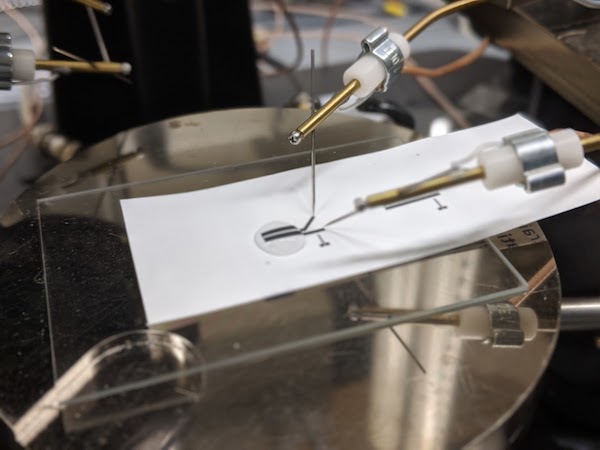
[Image above] Aarhus University assistant professor Shweta Agarwala holds up an example of a printed electronic. Credit: Shweta Agarwala, Aarhus University
When talking about additive manufacturing, we often imagine using these techniques to create large-scale 3D objects such as ceramic implants, turbine parts, or even homes. But by its nature, additive manufacturing excels at creating much less bulky devices as well, such as printed electronics.
“Printed electronics (PE) is an emerging technology under the umbrella of additive manufacturing that uses functional inks to print circuits and electrical components on various substrates,” researchers explain in a recent paper. “So far, PE has enabled fabrication of devices including but not limited to thin film solar cells, antennas, memories, transistors, displays, batteries, capacitors, and sensors.”
The researchers are led by Shweta Agarwala, assistant professor of electrical and computer engineering at Aarhus University (Denmark). She is joined by professor Preben Kidmose and Ph.D. student Hamed Abdolmaleki.
In an Aarhus press release, Abdolmaleki explains that compared to conventional lithography-based techniques for fabricating semiconductors, which use light to transfer a predefined pattern onto a rigid substrate, printed electronic techniques open “a plethora of new possibilities to print flexible electrical circuits directly onto a wide range of substrates such as plastics, papers, clothes, and quite literally any other planar and non-planar surfaces.”
Research on printed electronics is advancing quickly, so keeping abreast of the latest discoveries is challenging. “Through this paper, we have tried to fill the existing void in literature by discussing techniques, material inks, ink properties, post processing, substrates and application to provide a complete guide,” Agarwala says in the press release.
Below is a brief summary of the main findings from the 29-page review paper.
Types of printing processes
Printing processes can be broadly classified as “contact” and “noncontact.” In contact printing, ink is transferred directly from a patterned medium (such as an engraved roller or stencil) onto a substrate. In noncontact printing, ink droplets are ejected from a series of nozzles onto the intended surface.
The authors focus this review on the latter category of noncontact printing, which consists mainly of three droplet-based printing techniques: inkjet, aerosol‐jet, and electrohydrodynamic‐jet printing.
Inkjet technology is the most widely used noncontact method for printing electronics.
In this technique, ink droplets are ejected onto a substrate via either continuous inkjet or drop‐on‐demand ejection modes. In the former method, a continuous column of ink ejects from a nozzle and spontaneously splits into droplets due to an acoustic wave generated by a piezoelectric ceramic. In the latter method, ink droplets are ejected in a controlled manner by passing trigger signals through actuators (either thermal or piezoelectric) located within the printhead.
Compared to the other noncontact printing techniques, inkjet printers have fewer operating parameters and so can reach optimal printing conditions more easily and in less time.
Aerosol jet technology is relatively new compared to inkjet technology, yet researchers have already successfully used this technique to fabricate transistors, lithium-ion batteries, and solar cells, among other devices.
This technique involves formation and deposition of an aerosol on a substrate. “Aerosol” is defined as a suspension of liquid or solid particles in a gas carrier. While techniques to produce and deposit aerosols have been known since the mid‐20th century, only recently has the technology to control aerosol jet deposition by digital signals been developed.
Compared to the other noncontact printing techniques, aerosol jet printers have enhanced capabilities for printing complex designs on 3D substrates (rather than just planar substrates) and have relaxed requirements for ink rheology and fluid mechanic properties.
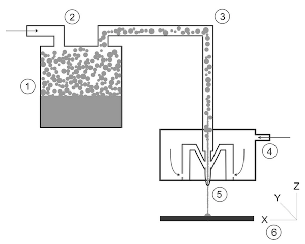
Electrohydrodynamic jet printing was patented in 1998 by Choi and Smith, but it wasn’t until 2007 that researchers at the University of Illinois at Urbana-Champaign significantly enhanced the resolution for printed electronics.
This technique uses an electric field to create fluid flow from the nozzle to the substrate. Flow rate and electrical field are two important parameters that determine the jetting behavior of inks. When these parameter values are low, droplets are ejected from the nozzle by gravitational forces in a “dripping” mode. As the values of these parameters increase, droplets are ejected in a “pulsating” mode and, at even higher values, a “cone-jet” mode.
Compared to the other noncontact printing techniques, electrohydrodynamic jet printers cater particularly to printing resolutions smaller than 100 nm, which is promising for printing cells and tissues for biotechnology and biomedical applications.
Types of functional inks
To date, researchers have explored several kinds of organic and inorganic materials for printed electronics. While organic materials show better flexibility and processibility, inorganic materials often possess better electrical properties.
A functional ink typically has four constituents:
- Solvent—The solvent dissolves or disperses the other three constituents and tunes the ink’s final viscosity.
- Functional material—The functional material endows the ink with electrical properties.
- Polymer binder—The polymer binder minimizes intermolecular interactions between nanoparticles, thus increasing the ink’s stability and shelf life.
- Additives—The additives enhance stability and performance. The most widely used additives are dispersing agents (surfactants), rheology modifiers, defoamers, plasticizers, and biocides.
In terms of functional materials, inks can be classified into four main categories: metal inks, carbon‐based inks, polymer inks, and ceramic inks.
For metal inks, silver is the most widely used functional material due to its outstanding electrical conductivity and high chemical resistance. Gold, though expensive, is used as well due to its high functionality and superior chemical stability, which makes it a preferred choice for applications involving corrosive and extreme environments. Copper is considered a low-cost alternative to silver and gold, but it can undergo rapid oxidation when exposed to ambient oxygen and thus is difficult to handle.
For carbon-based inks, graphene and carbon nanotubes are widely used. Graphene inks are prepared using four main approaches: oxidative exfoliation, sonication‐induced exfoliation, shear exfoliation, and electrochemical exfoliation. Preparing carbon nanotube-based inks is difficult because of the material’s poor dispersion in water and organic solvents, but researchers have devised several physical and chemical strategies for overcoming this challenge, such as using different dispersants or surface modification techniques.
Polymer inks are of high interest due to excellent mechanical compliance and easy processability via solution‐based methods. There are two main classes of functional polymers: conjugated polymers and electroactive polymers. In general, conjugated polymers show poor device performance and low charge carrier mobility due to their semicrystalline nature. In contrast, electroactive polymers are highly sought after due to their ability to change size and shape in response to an electrical field, which is a useful characteristic for fabricating sensors and actuators.

Ceramic inks can show interesting electrical properties, such as superconductivity, semiconductivity, piezoelectricity, and magnetic features. For ceramic inks to yield a uniform pattern when printed, they should fulfill three main requirements: 1) adequate particle size and stability of the suspension, 2) proper fluid mechanics, and 3) proper drying behavior.
Limiting factors and challenges
After reviewing post-processing methods and types of substrates, which you can read more about in the paper, the authors conclude by detailing some areas in which research and innovation are needed to push this emerging technology toward commercialization. For example,
- Printability—Printability is the ability of a final product to follow the initial computer designed pattern. However, most of the software used for printed electronics have constraints on curved edges or multilayer designs, which restricts the design possibilities. In addition, due to fluid mechanic requirements, the viscosity and solid content of inks cannot exceed a certain value, meaning many printing passes may be required to achieve a thicker printed pattern.
- Device fabrication—An encapsulation layer is typically used to protect printed electronics, which are prone to damage due to their thin and flexible nature. However, challenges with choosing an encapsulation layer include elastic constant mismatch, thermal expansion mismatch, and stress concentration from the layer to the printed circuit.
The paper, published in Advanced Materials, is “Droplet‐based techniques for printing of functional inks for flexible physical sensors” (DOI: 10.1002/adma.202006792).