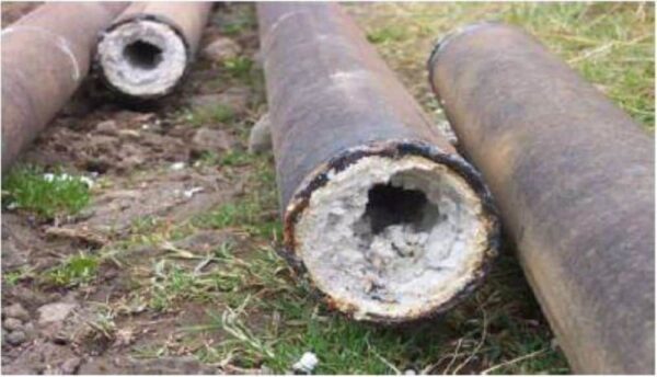
[Image above] The reaction of silica with positive ions like calcium and magnesium lead to formation of insoluble silica “scales” (pictured above) that foul up equipment. Ceramic nanofiltration membranes can help remove compounds like dissolved silica from wastewaters so silica scale formation is avoided. Credit: Wardana et al., IOP Conference Series: Earth and Environmental Science (CC BY 3.0)
With passage of the CHIPS and Science Act of 2022 in August, semiconductor manufacturers are rallying for their share of the funds. But even as they break ground on new fabrication facilities, environmental impacts remain top of mind for many viewing the construction.
To the industry’s credit, many chip manufacturers are innovating and investing across their operations to make production more sustainable. For example, Intel, which just started construction of a new semiconductor mega-site in Ohio, uses renewable energy for 82% of its global operations as of its most recent reports.
Water recycling is another approach companies take to lower their environmental impact. A typical semiconductor manufacturing facility uses two to four million gallons of ultrapure water per day; some large facilities can use close to 10 million gallons. Thus, many companies invest in filtering technologies to reduce the amount of outside water needed to operate the plant.
Filtering semiconductor wastewater is no easy task. It contains a wide range of organic and inorganic impurities removed during the manufacturing process, such as hydrofluoric acid, phosphoric acid, ammonium hydroxide, photoresists, and strippers.
Currently, membrane-related filtering processes, which are based on the physical separation of solutes, are a research focus because they are easily implemented and scaled-up without the need for chemical additives and phase changes. However, while researchers have investigated the use of ceramic membranes to treat some types of wastewaters due to their high chemical, thermal, and structural stability, these membranes are not widely investigated for semiconductor wastewater treatment specifically.
Chanhyuk Park, associate professor of environmental science and engineering at Ewha Womans University (Seoul, South Korea), is changing that paradigm. In February, we covered a study by his group investigating the potential of graphene oxide-based nanofiltration membranes to remove ammonium from semiconductor wastewater. Now, they and a colleague from the Korea Institute of Materials Science published a new paper on the potential of functionalized boron nitride-based nanofiltration membranes to remove colloidal and dissolved silica.
Highly alkaline silica is used in the chemical mechanical polishing process for planarizing semiconductor wafers. Incorrect treatment of colloidal and dissolved silica in the wastewater leads to the reaction of silica with positive ions like calcium, magnesium, iron, manganese, and aluminum, forming insoluble silica “scales” that foul up equipment.
Nanofiltration membranes can remove compounds like dissolved silica with a relatively low molecular weight because the membrane’s charge and size exclusion mechanisms favor the retention of contaminants. To further improve their separation performance, researchers currently are exploring modification of the membrane’s surface using 2D nanomaterials, such as titanium dioxide, graphene oxide, and boron nitride.
So far, researchers have only explored using boron nitride to functionalize polymeric membranes. However, the polymer base exhibits poor durability under harsh chemical conditions, such as acidic and basic solutions. Thus, “The combination of h-BN [hexagonal boron nitride] nanomaterials and ceramic membranes could significantly improve membrane separation performance,” Park and his coauthors write.
In the new study, they used functionalized h-BN to modify a commercially available titanium dioxide-based ceramic ultrafine membrane. They then compared these modified membranes to some original, unmodified ones to determine if separation performance improved.
Testing revealed that the h-BN coating improved both the particulate and organic contaminant separation efficiency of the membrane. Specifically, compared to the unmodified membranes, the functionalized h-BN-coated membranes increased rejection of dissolved silica and humic acid by 20.4% and 59.8%, respectively.
Based on these results, “Additional treatment with the [h-BN-coated membranes] after filtration through the ceramic [ultrafine] membrane could be an attractive and efficient approach for maintaining dissolved silica concentrations below the solubility limits and meeting the discharge limit of [total organic carbon] concentration during semiconductor wastewater treatment,” they conclude.
They write that future studies should investigate the long-term stability of the membranes under various operating conditions, including tests with real semiconductor wastewaters, to expand its range of uses.
The paper, published in Separation and Purification Technology, is “Functionalized boron nitride ceramic nanofiltration membranes for semiconductor wastewater treatment” (DOI: 10.1016/j.seppur.2022.121945).