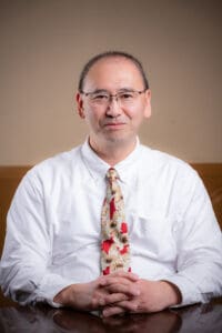
Kiyoshi Shimamura

Field Director, Optical Materials Field
Group Leader, Optical Single Crystals Group
Research Center for Functional Materials
National Institute for Materials Science (NIMS)
E-mail: SHIMAMURA.Kiyoshi@nims.go.jp
Title : Novel single crystals for electro-optical applications
Electro-optical technology progress in a wide range of applications, and still demands the further development. Our intention is to explore novel single crystal materials for diverse applications, and to implement them in the industrial use.
β-Ga2O3 single crystal was proposed as a brandnew wide-gap (Eg = 4.8 eV) semiconductor in 2001. 2 inch size β-Ga2O3 single crystals were grown by the EFG technique. Shotky barrier diode of it was demonstrated in 2009. Since then, tremendous considerations for the industrial implementation have been on going.
A new concept of high-brightness white LED/LDs based on Ce: Y3Al5O12 (YAG) single crystal phosphor plates (SCPPs), which can overcome the conventional temperature- and photo-degradation problems, has been proposed. SCPPs demonstrated excellent thermal stability, high values of luminous efficacy and increased quantum efficiency. The implementation has started in 2017.
Tb3(Sc1-xLux)2Al3O12 (TSLAG) single crystals have been designed for high-power laser machinery. It showed a higher visible transparency and a larger Faraday rotation than the conventional Tb3Ga5O12 (TGG). In 2013, mass production has started.
A drastic enhancement of the light yield of Ce:Li6Y(BO3)3 (LYBO) single crystals by ∼600% is achieved. Ce:LYBO could be of interest as efficient, low-cost, and stable solid-state materials for portable thermal neutron detection.
Kiyoshi Shimamura graduated in Applied Chemistry at Waseda University, Japan, and took his Ph.D. in Chemistry at Tohoku University, Japan, in 1995. He is a Field Director of Optical Materials Field, Research Center for Elctronic and Optical Materials, National Institute for Materials Science (NIMS). His research interests deal with the design, growth, and characterization of novel single crystal materials mainly for optical, piezoelectric, and semiconductor applications. A point worthy to mention is that he performs the research toward social implementation though his research is based on fundamental research.
He was visiting researcher at Institut de Chimie de la matière condensée de Bordeaux – Centre national de la recherche scientifique ICMCB-CNRS, France. He is now visiting professor at Graduate School of Advanced Science and Engineering, Waseda University, Japan. Also, he is now CEO of E-Crystal Inc., formed in 2015 from NIMS. He is promoting joint research with companies, and supervising Ph.D. students and post-doc researchers. He is involved in several Japanese Associations and ACerS activities. Since 2024, he is a chair of Japan Chapter, ACerS. He has co-authored 299 papers in peer-reviewed journals.
Subscribe to Ceramic Tech Today

Don’t miss the latest ceramic and glass materials news. Receive the CTT newsletter to your email three times a week by subscribing at this link.
Subscribe to Ceramic & Glass Manufacturing Weekly

Don’t miss the latest ceramic and glass business news. Receive the C&GM Weekly newsletter to your email every Monday by subscribing at this link.


