By processing samples of silicon nitride under high pressure and heat, researchers at the Deutsches Elektronen-Synchrotron have converted an originally opaque hexagonal crystal structure into optically transparent cubic silicon nitride.
Read More
Researchers at Colorado School of Mines and the University of Florida are well on their way to solving grain boundaries’ secrets—the team recently achieved unprecedented atom-by-atom visualization of the chemical composition of grain boundaries.
Read More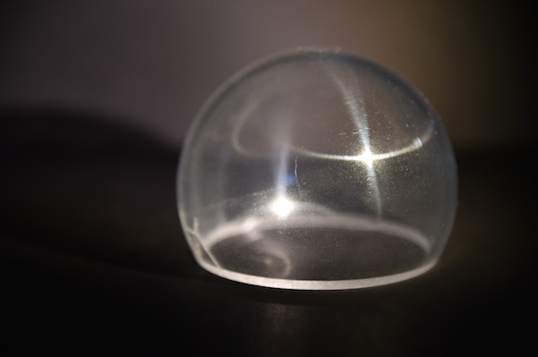
U.S. Naval Research Lab scientists have perfected a sintering technique that can not only produce harder spinel, but also larger pieces and those with challenging shapes—all thanks to a deconstruction of the science behind the process.
Read MoreWhen you are in the solar cell business (polycrystalline silicon) or semiconductor business (monocrystalline), silicon ingots and boules – the source of your vital wafers – can be a considerable…
Read MoreKudos to Akio Ikesue and Yan Lin Aung for their recent article in Nature Photonics. Ikesue (bias confession: he is an ACerS member) and Yan report on recent developments in…
Read More